Capacitor and Method for Manufacturing the Same

a capacitor and electrode technology, applied in the field of capacitors, can solve the problems that the resistance of the capacitor electrode is limited by the crystal or polycrystalline silicon, and achieve the effect of reducing leakage currents and high density capacitan

Inactive Publication Date: 2010-07-01
DONGBU HITEK CO LTD
View PDF4 Cites 7 Cited by
  • Summary
  • Abstract
  • Description
  • Claims
  • Application Information

AI Technical Summary

Benefits of technology

[0010]Embodiments of the present invention enable reduction of the thickness of the capacitor, and provide a capacitor including a dielectric layer having a high permittivity.
[0015]A capacitor according to the present invention comprises a dielectric layer that uses silicon oxide layers and a zirconium-doped hafnium oxide (Zr-doped HfO2) layer. As a result, a low VCC voltage may be useable, and leakage currents may be reduced such that a thin film device having a high density capacitance may be provided.

Problems solved by technology

However, such single-crystal or polycrystalline silicon has limitations in reducing the resistance of the capacitor electrodes because of the material characteristics.

Method used


Image

  • Capacitor and Method for Manufacturing the Same
  • Capacitor and Method for Manufacturing the Same
  • Capacitor and Method for Manufacturing the Same

Examples


Embodiment Construction

[0019]Reference will now be made in detail to various embodiments of the present invention, examples of which are illustrated in the accompanying drawings. Wherever possible, the same reference numbers will be used throughout the drawings to refer to the same or like parts.

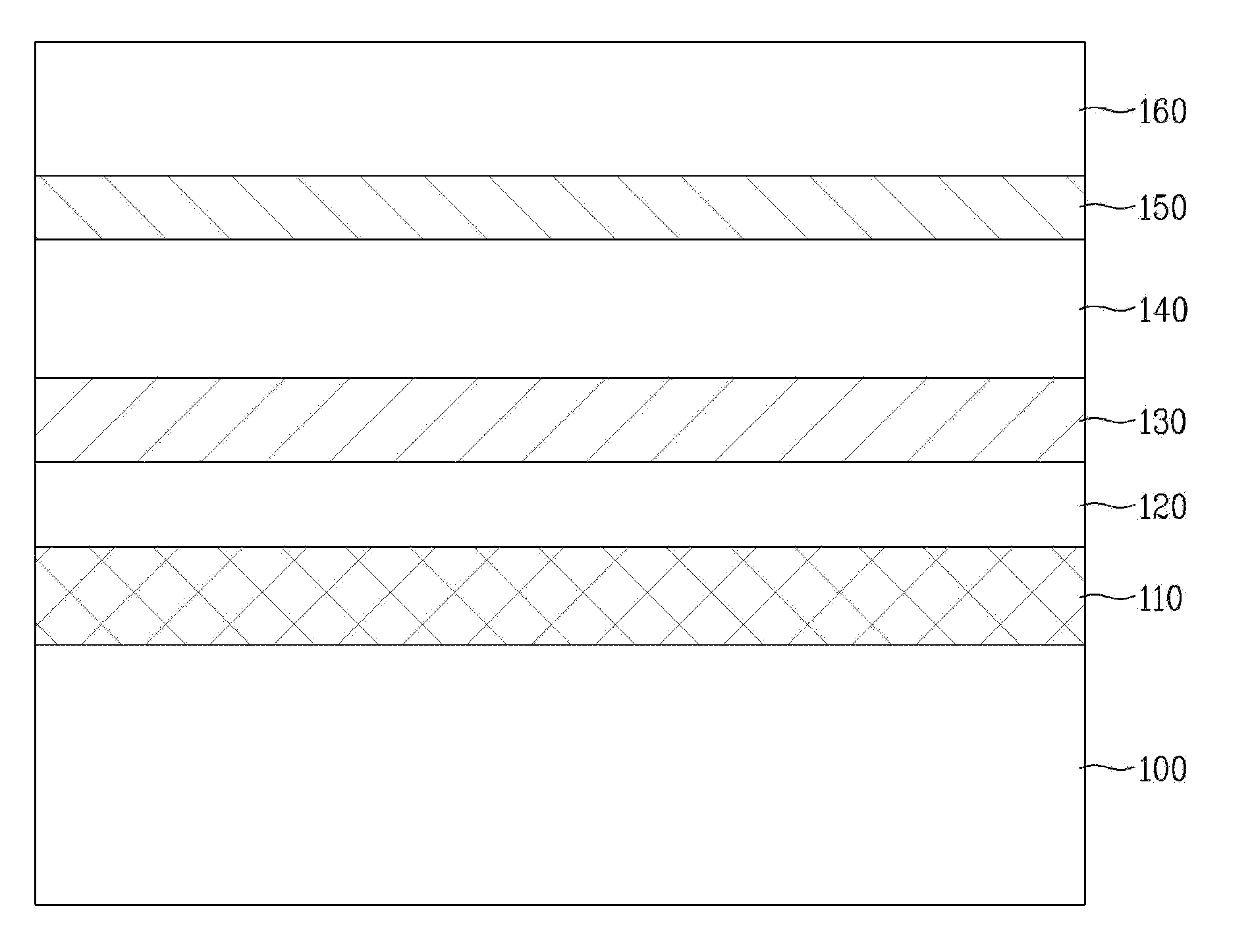
[0020]A capacitor according to exemplary embodiments will be now described with reference to FIG. 1.

[0021]As shown in FIG. 1, a capacitor according to exemplary embodiments of the present invention may include an insulation layer 110 formed on a substrate 100, a first electrode 120, first silicon oxide layer 130, a Zr-doped HfO2 layer 140, second silicon oxide layer 150 and second electrode 160.

[0022]The first and second silicon oxide layers (SiO2) 130 and 150 are generally deposited to a thickness of about 1 nm˜2 nm with a Zr-doped HfO2 layer 140 disposed therebetween. The silicon oxide layers 130 and 150 and the Zr-doped HfO2 layer are used as a dielectric layer. As a result, a low VCC voltage may be employed, a...


PUM

PropertyMeasurementUnit
thicknessaaaaaaaaaa
thicknessaaaaaaaaaa
temperaturesaaaaaaaaaa

Abstract

A capacitor and methods for manufacturing the capacitor are disclosed. The method may include forming a first electrode on a substrate, forming a dielectric layer on the first electrode, the dielectric layer having a first silicon oxide (SiO2) layer, a zirconium-doped hafnium oxide (Zr-doped HfO2) layer and a second silicon oxide layer sequentially, and forming a second electrode on the dielectric layer.

Description

CROSS REFERENCE TO RELATED APPLICATION[0001]This application claims the benefit of Korean Patent Application No. 10-2008-0138083, filed on Dec. 31, 2008, which is hereby incorporated by reference as if fully set forth herein.BACKGROUND OF THE DISCLOSURE[0002]1. Field of the Disclosure[0003]The present invention relates to a semiconductor device, more particularly, to a capacitor and a method for manufacturing the capacitor.[0004]2. Discussion of the Related Art[0005]As usage of semiconductor devices has increased, demands for fast and large-sized capacitors have also been increasing. For such a fast capacitor, the resistance of the capacitor electrodes is typically reduced to reduce the frequency dependence of the capacitor. For a large-sized capacitor, the thickness of a dielectric substance between the capacitor electrodes is reduced, a material having a high permittivity is used as dielectric layer, or an area of the capacitor electrodes is increased.[0006]A capacitor used in a s...

Claims


Application Information

Patent Timeline
Patent Type & Authority Applications(United States)
IPC IPC(8): H01L29/92H01L21/02
CPCH01L21/02181H01L21/02189H01L21/02194H01L21/022H01L21/31645H01L28/40H10B99/00H10B12/00
Inventor KIM, HYUN DONG
Owner DONGBU HITEK CO LTD
Why Eureka
Try Eureka