
Imprint process of thermosetting material

a thermosetting material and imprinting technology, applied in patterning and lithography, printed circuit manufacturing, lithography/patterning, etc., can solve the problems of large amount of laser energy, increased cost, and the inability of laser machining technology to produce patterns with too small sizes, so as to increase the accuracy and reliability of pattern transfer

Inactive Publication Date: 2010-07-08
NAT CHENG KUNG UNIV
View PDF32 Cites 6 Cited by
  • Summary
  • Abstract
  • Description
  • Claims
  • Application Information

AI Technical Summary

Benefits of technology

[0009]Therefore, one objective of the present invention is to provide an imprint process of a thermosetting material, which can accurately transfer a pattern on an imprint mold to a thermosetting material layer, thereby effectively increasing the accuracy and the reliability of the pattern transferred to the thermosetting material layer.
[0010]Another objective of the present invention is to provide an imprint process of a thermosetting material, which can successively define the pattern of the thermosetting material with low thermal budget and under relatively lower temperatures compared with the hot embossing nanoimprint process, thereby reducing the process cost and preventing the feature size of the transferred pattern of the thermosetting material from being distorted. Furthermore, the remaining thermal stress formed on the substrate and the thermosetting material layer due to high temperature can be decreased, and the substrate and the thermosetting material layer can be prevented from being damaged.

Problems solved by technology

However, when the laser machining technology patterns the thermosetting material, irradiation of many laser shots is required, so that the process is time-consuming and consumes large amounts of laser energy, thereby increasing the cost.
Moreover, due to the size of the laser beam and the optical diffraction limit, the laser machining technology cannot produce the pattern with too small size, such as the thermosetting material pattern structures with the nanometer scale.
However, due to the wavelength limit of the exposure light source, the feature size of the thermosetting material pattern strictures produced by the conventional photolithography technology has a limit, so that the pattern structures with a smaller size cannot be produced.
However, the surface roughness of the thermosetting material pattern structure formed by the new photolithography technology is poor, there still exists many issues in the positive tone and negative tone photosensitive thermosetting materials, such as that the adjustment of the ingredients of the material is difficult, and the control of the process parameters and the machining precision of the thermosetting material is difficult to result in the poor fidelity and the reliability of pattern transferring.
In addition, similarly, due to the wavelength limit of the exposure light source, the new photolithography technology cannot produce the thermosetting material pattern structures with a smaller size.
Furthermore, the negative tone photosensitive thermosetting material is swelling after the developing process, so that the fidelity of the pattern transferring is further decreased.
Therefore, the surface of the pattern structures of the thermosetting material formed by the soft nanoimprint technology has many holes, so that the surface roughness of the thermosetting material pattern structures is poor, and the mechanical strength of the thermosetting material pattern structures is reduced.
In addition, due to the heat, the remaining thermal stress, the expansion and the shrink effects occur on the mold and the substrate simultaneously, thereby seriously affecting the substrate material and the size of the thermosetting material pattern structures to reduce the reliability of the pattern transferring.

Method used


Image

  • Imprint process of thermosetting material
  • Imprint process of thermosetting material
  • Imprint process of thermosetting material

Examples


Embodiment Construction

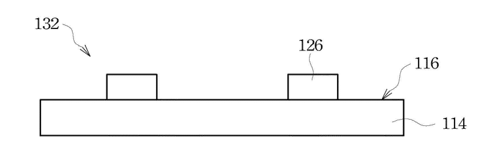
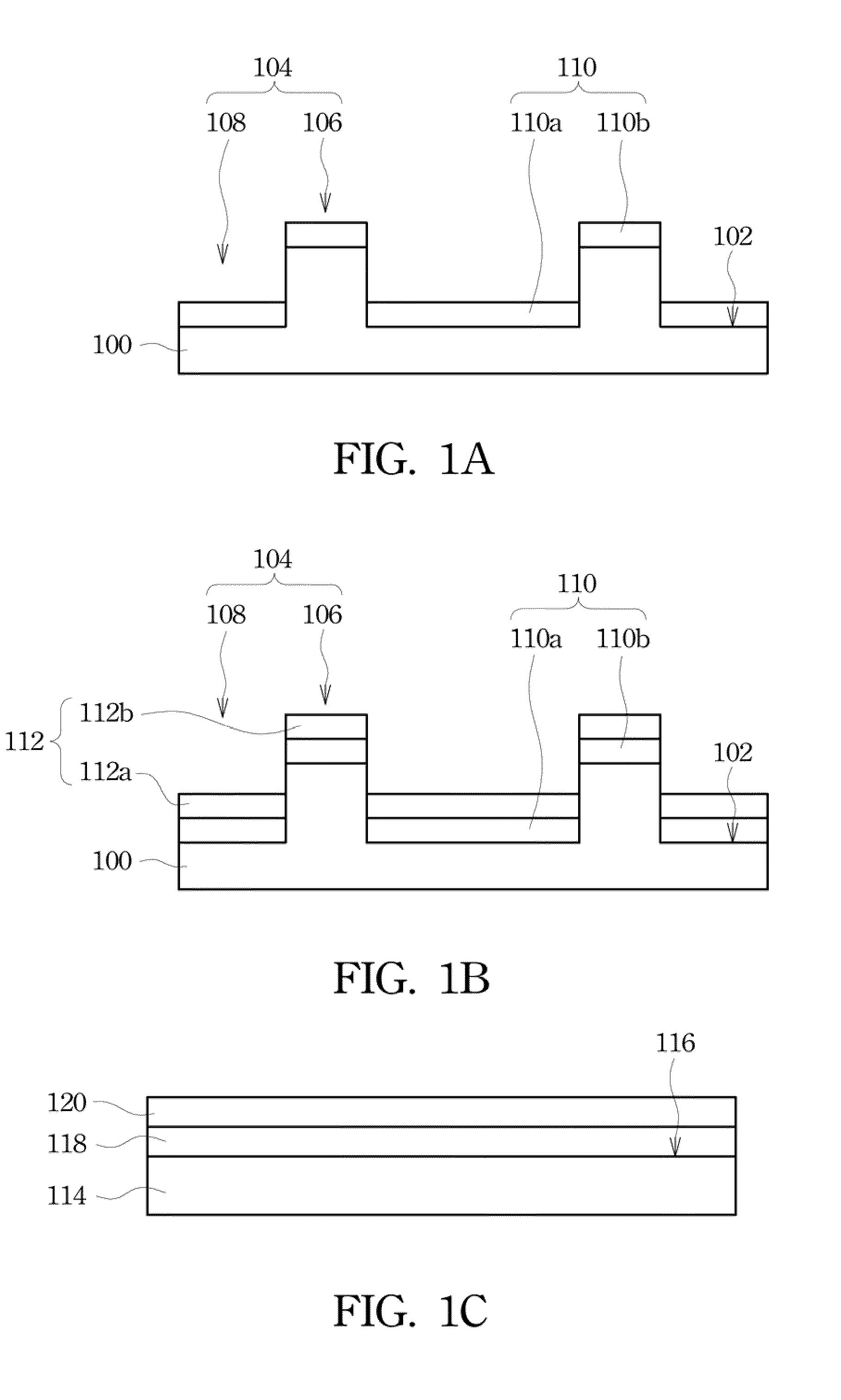
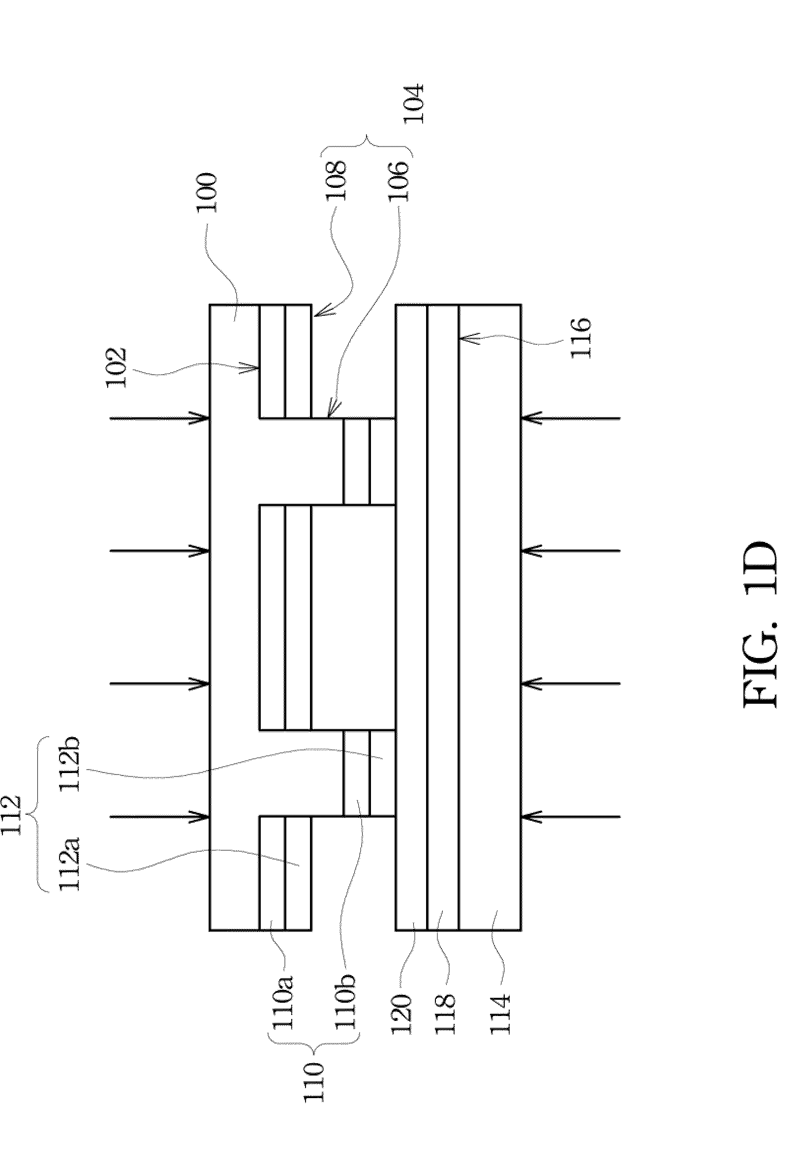
[0015]FIGS. 1A through 1H are schematic flow diagrams showing an imprint process of a thermosetting material in accordance with a preferred embodiment of the present invention. In an exemplary embodiment, when the imprint process of a thermosetting material is performed, a mold 100 may be provided to perform the imprint process. A pattern structure 104 is set in a surface 102 of the mold 100, wherein the pattern structure 104 comprises a plurality of concave portions 108 and a plurality of convex portions 106. The feature size of the pattern structure 104 may be micrometer scale or nanometer scale. Next, such as shown in FIG. 1A, an anti-stick layer 110 is selectively formed to cover the pattern structure 104 of the mold 100 by, for example, a thermal evaporation method, wherein the anti-stick layer 110 includes two portions 110a and 110b, the portion 110a of the anti-stick layer 110 covers on bottoms of the concave portions 108 of the pattern structure 104, and the portion 110b of ...


PUM

PropertyMeasurementUnit
Temperatureaaaaaaaaaa

Abstract

An imprint process of a thermosetting material is described, comprising: providing a mold including pattern structures, wherein convex portions and concave portions of the pattern structures are covered with a transferred material layer; providing a substrate, wherein a thermosetting material layer and a sacrificial layer cover the substrate in sequence; performing an imprint step to transfer the transferred material layer on the convex portions onto a first portion of the sacrificial layer; etching a second portion of the sacrificial layer and the underlying thermosetting material layer by using the transferred material layer as a mask; and performing a wet stripping step by using a stripper to completely etch the sacrificial layer and the overlying transferred material layer, wherein the stripper has a first etching rate and a second etching rate to the thermosetting material layer and the sacrificial layer respectively, and a ratio of the second etching rate to the first etching rate is greater than or equal to 30.

Description

RELATED APPLICATIONS[0001]This application claims priority to Taiwan Application Serial Number 98100535, filed Jan. 8, 2009, which is herein incorporated by reference.FIELD OF THE INVENTION[0002]The present invention relates to an imprint process, and more particularly to an imprint process of a thermosetting material.BACKGROUND OF THE INVENTION [0003]A thermosetting material, such as polyimide (PI), is a material with high heat resistance, a great mechanical property, a superior optical property and a low dielectric constant, so that the thermosetting material has been widely applied in flexible printed circuit (FPC) boards, electronic packages, optical waveguides, alignment films of liquid crystal displays (LCD) and microfluidic devices. In the application, the thermosetting material typically needs to be patterned by a pattern definition technology to form the desired pattern structure for use.[0004]Several technologies, such as laser machining technology, conventional photolitho...

Claims


Application Information

Patent Timeline
IPC IPC(8): B44C1/22
CPCH05K3/002H05K2203/0108H05K2203/0537H05K2203/308
Inventor LEE, YUNG-CHUNCHIU, CHENG-YULEE, CHUNG-YI
Owner NAT CHENG KUNG UNIV
Learn More