Surface emitting laser, surface emitting laser array, optical scanning device,image forming apparatus, optical transmission module and optical transmission system

Active Publication Date: 2010-07-29
RICOH KK
View PDF34 Cites 22 Cited by
  • Summary
  • Abstract
  • Description
  • Claims
  • Application Information

AI Technical Summary

Benefits of technology

[0032]The present invention is made based on the findings that the inventors et al. have obtained. A first object of the present invention is to provide a surface emitting laser and a surface emitting laser array that may be easily manufactured, have higher yield, and have a longer service lifetime.
[0054]By having this, since the optical transmission system includes an optical transmission module according to an embodiment of the present invention, it becomes possible to perform high-quality optical data transmission.

Problems solved by technology

However, unfortunately, in surface emitting lasers having an oxide-confined structure, due to a large refractive index difference in the lateral direction caused by the oxidized layer, an even higher-order lateral mode may also be confined and oscillated.
Especially, as described above, when the size of the confined region is reduced, the size of the oscillation region becomes accordingly smaller, which makes it difficult to obtain high power and makes the resistance of the surface emitting laser larger.
However, unfortunately, in the surface emitting laser disclosed in Patent Document 2, the lateral mode characteristics, the output, and the like are extremely susceptible to the size of an electrode opening, the displacement between the electrode aperture and the selected oxidation structure, and the like.
Because of the disadvantage, high alignment accuracy and high shape controllability for fabrication become necessary, which makes it difficult to uniformly manufacture surface emitting lasers.
In addition, severe process control needs to be performed, which results in the increase of the manufacturing cost.
Further, the surface emitting laser disclosed in Patent Document 3 requires processes of forming a dielectric film and partially removing the dielectric film, which disadvantageously increases the manufacturing cost.
Additionally, the device characteristics are susceptible to the accuracy of the displacement between the dielectric film and the current injection region, which makes it difficult to uniformly manufacture the surface emitting lasers.
On the other hand, when one of the plural low refractive index layers in a semiconductor multilayer film reflection mirror is entirely a selectively-oxidized layer (as described in, for example, Patent Document 1 and Patent Document 4), the thickness of the oxidized layer becomes in a range from 50 nm to 80 nm, which may cause large distortion due to volume shrinkage caused by the oxidation.
However, the oxidized layer may serve as a main component accelerating the degradation due to the distortion, and there is a tendency that the thicker the oxidized layer is, the faster the degradation proceeds.
Therefore, the oxidized layer becomes thicker and the distortion due to volume shrinkage caused by the oxidation may negatively affect the active layer and accelerate the degradation of the characteristics.
Further, in the surface emitting laser disclosed in Patent Document 1 and Patent Document 4, when viewed from the active layer, the current confined layer is located between the node and the antinode positions of the electric field intensity distribution, which disadvantageously increases the diffraction loss and reduces the single mode output.
However, unfortunately, in the oxide-confined VCSEL disclosed in Patent Document 5, the oxide aperture forming layer (corresponding to the current confined structure) and the transition layer (corresponding to the composition gradient layer) adjoin each other.
Therefore, it is difficult to locate both of the layers at a node position of the electric field intensity distribution at the same time.
Therefore, the device characteristics of the single-mode devices are likely to be more severely affected by the variation of the oxidation amount in the selectively-oxidized layer.
Especially, when the size of the current injection region becomes larger than desired, the device may be operated in multi-mode and the yield of manufacturing single-mode devices is disadvantageously reduced.

Method used


Image

  • Surface emitting laser, surface emitting laser array, optical scanning device,image forming apparatus, optical transmission module and optical transmission system
  • Surface emitting laser, surface emitting laser array, optical scanning device,image forming apparatus, optical transmission module and optical transmission system
  • Surface emitting laser, surface emitting laser array, optical scanning device,image forming apparatus, optical transmission module and optical transmission system

Examples


first embodiment

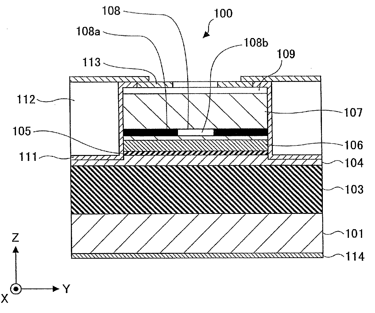
[0144]FIG. 1 is a cross-sectional diagram schematically showing a surface emitting laser 100 according to a first embodiment of the present invention. It should be noted that the Z-direction in the figures is the direction parallel to the laser oscillation direction, and X-direction and Y-direction are orthogonal to each other and in the plane orthogonal to the Z-direction.

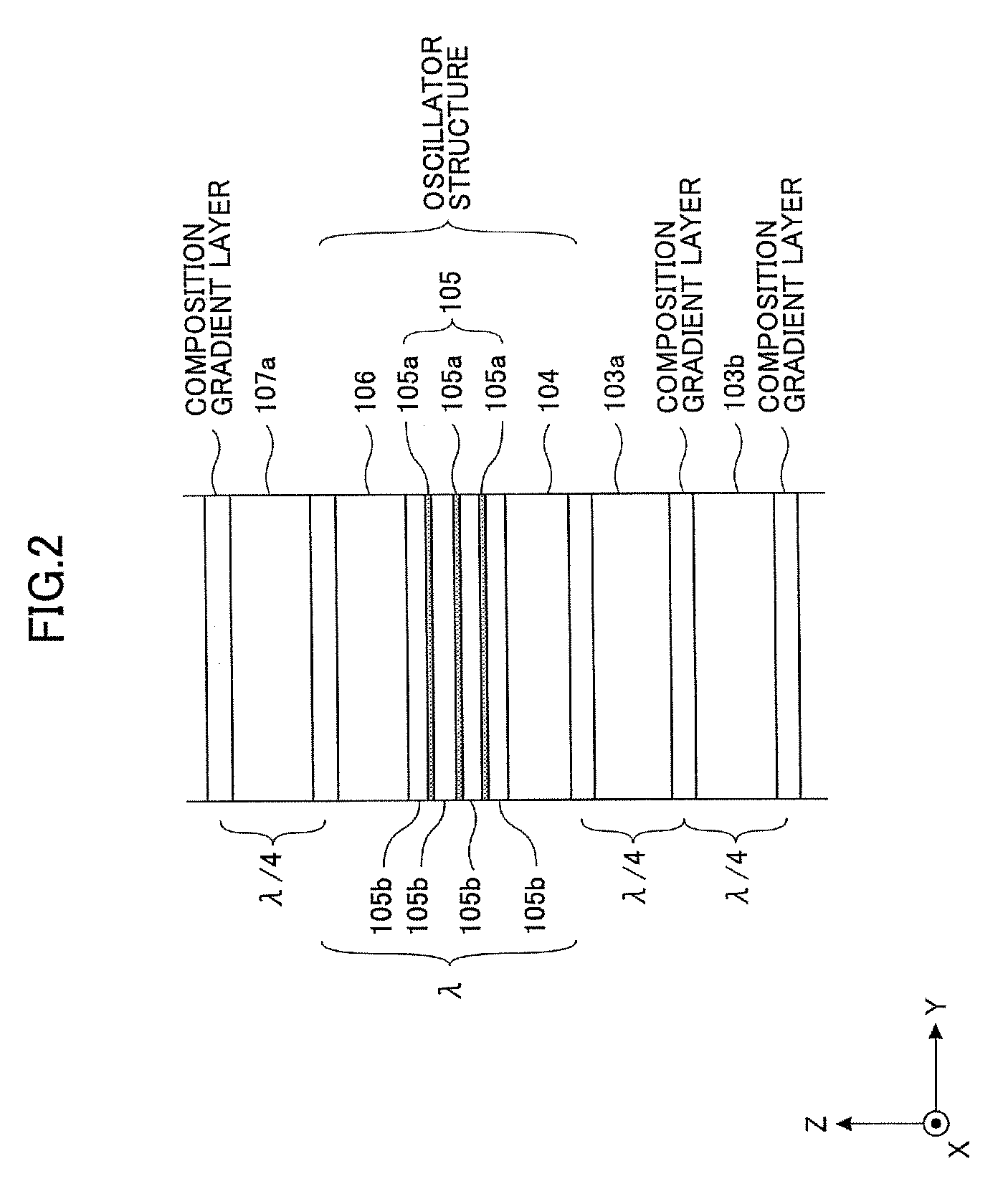
[0145]The surface emitting laser 100 is designed to oscillate at the wavelength band of 850 nm. As shown in FIG. 1, in the surface emitting laser 100, a lower semiconductor DBR 103, a lower spacer layer 104, an active layer 105, an upper spacer layer 106, an upper semiconductor DBR 107, and a contact layer 109 are sequentially laminated in this order on a substrate 101. In the following, it should be noted that a laminated structure including plural semiconductor layers may be called a “laminated body” for convenience. FIG. 2 is an enlarged view of the vicinity of the active layer 105, and FIG. 3 is a partially-en...

second embodiment

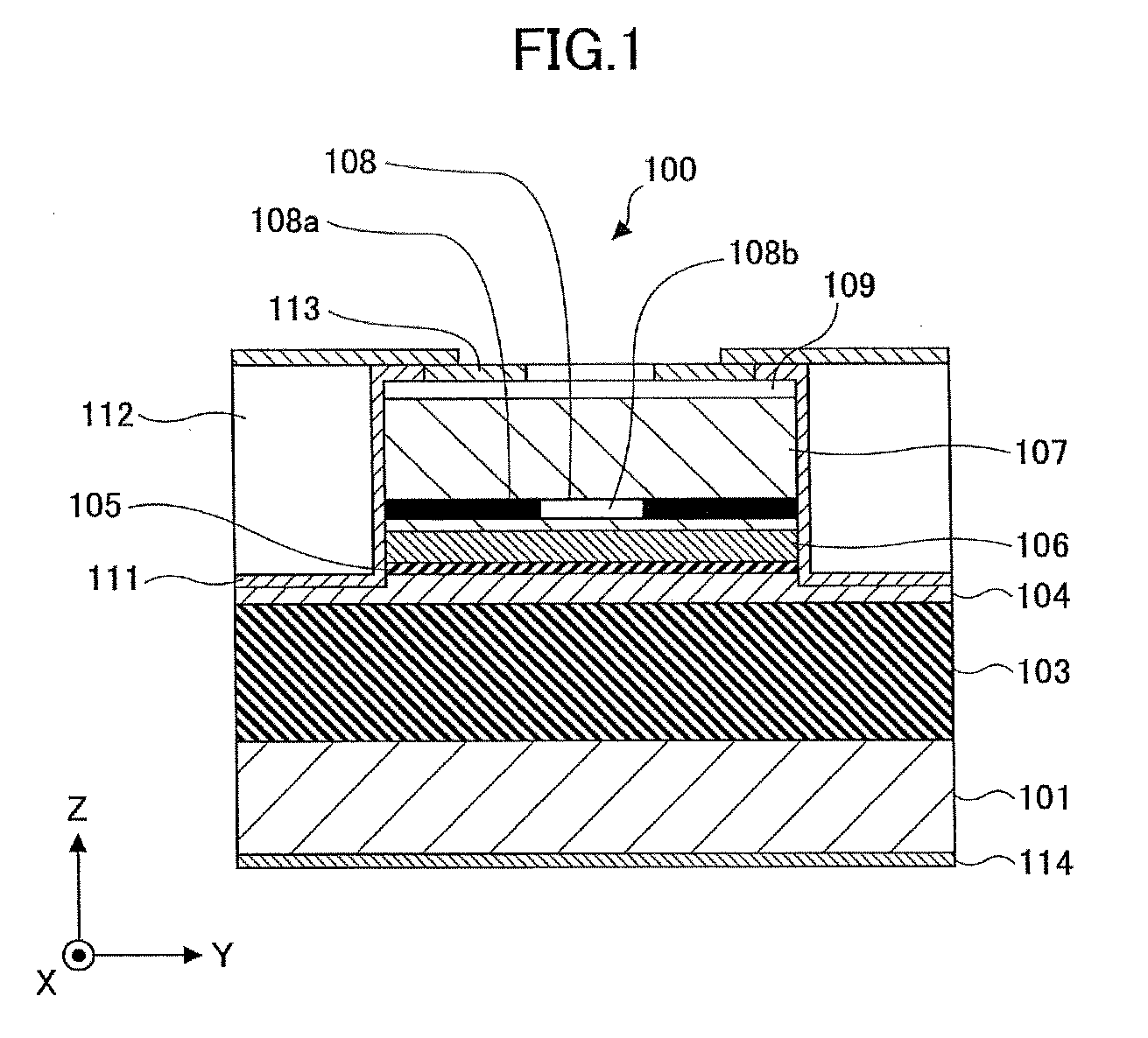
[0194]FIG. 1 is a cross-sectional diagram schematically showing a surface emitting laser 100 according to a second embodiment of the present invention.

[0195]The surface emitting laser 100 is designed to oscillate at the wavelength band of 780 nm. As shown in FIG. 1, the surface emitting laser 100 includes semiconductor layers such as a substrate 101, a lower semiconductor DBR 103, a lower spacer layer 104, an active layer 105, an upper spacer layer 106, an upper semiconductor DBR 107, and a contact layer 109, laminated with each other. In the following, it should be noted that a laminated structure including plural semiconductor layers may be called a “laminated body” for convenience. FIG. 2 is an enlarged view of the vicinity of the active layer 105, and FIG. 7 is a partially-enlarged view of the upper semiconductor DBR 107.

[0196]The substrate 101 is a single-crystal substrate made of n-GaAs.

[0197]The lower semiconductor DBR 103 includes 40.5 pairs of a low refractive index layer 1...

third embodiment

[0250]FIG. 17 schematically shows a configuration of a surface emitting laser 200 according to a third embodiment of the present invention.

[0251]The surface emitting laser 200 is designed to oscillate at the wavelength band of 780 nm. As shown in FIG. 17, in the surface emitting laser 200, a lower semiconductor DBR 203, a lower spacer layer 204, an active layer 205, an upper spacer layer 206, an upper semiconductor DBR 207, and a contact layer 209 are sequentially laminated in this order on a substrate 201. FIG. 18 is an enlarged view of the vicinity of the active layer 205, and FIG. 19 is a partially-enlarged view of the upper semiconductor DER 207.

[0252]The substrate 201 is a single-crystal substrate made of n-GaAs.

[0253]The lower semiconductor DBR 203 includes 40.5 pairs of a low refractive index layer 203a made of n-AlAs and a high refractive index layer 203b made of n-Al0.3Ga0.7As. Further, a composition gradient layer is interposed between the adjacent refractive index layers ...


PUM


Abstract

A disclosed surface emitting laser is capable of being manufactured easily, having a higher yield and a longer service lifetime. In the surface emitting laser, a selectively-oxidized layer is included as a part of a low refractive index layer of an upper semiconductor distribution Bragg reflector; the low refractive index layer including the selectively-oxidized layer includes two intermediate layers adjoining the selectively-oxidized layer and two low refractive index layers adjoining the intermediate layers. Al content rate in the intermediate layers is lower than that in the selectively-oxidized layer, and Al content rate in the low refractive index layers is lower than that in the selectively-oxidized layer. This configuration enables providing more control over the thickness and oxidation rate of the oxidized layer, thereby enabling reducing the variation of the thickness of the oxidized layer.

Description

TECHNICAL FIELD[0001]The present invention relates to a surface emitting laser, a surface emitting laser array, an optical scanning device, an image forming apparatus, an optical transmission module, and an optical transmission system. More specifically, the present invention relates to a surface emitting laser emitting light in the direction perpendicular to its substrate, a surface emitting laser array having plural surface emitting lasers, and an optical scanning device, an image forming apparatus, an optical transmission module, and an optical transmission system, each having the surface emitting laser array.BACKGROUND ART[0002]A Vertical Cavity Surface Emitting Laser (hereinafter may be referred to as “VCSEL”) is a semiconductor laser that emits light in the direction perpendicular to its substrate. When compared with edge emitting semiconductor lasers, the VCSEL has some advantages including (1) lower cost, (2) lower energy consumption, (3) smaller sizes, and (4) easier to per...

Claims


Application Information

Patent Timeline
IPC IPC(8): G03G15/04H01S5/183H01S5/187H01S5/42
CPCB41J2/45H01S5/0021H01S5/423H01S5/18358H01S5/18313
Inventor SATO, SHUNICHIITOH, AKIHIROHINO, TAKESHIJIKUTANI, NAOTO
Owner RICOH KK
Why Eureka
Try Eureka