

Method for depositing silicon nitride films and/or silicon oxynitride films by chemical vapor deposition
a technology of silicon oxynitride and silicon nitride, which is applied in the direction of chemical vapor deposition coating, coating, metallic material coating process, etc., can solve the problems of low film density, high etch rate, and inability to achieve commercially acceptable film formation rate,
- Summary
- Abstract
- Description
- Claims
- Application Information
AI Technical Summary
Benefits of technology
Problems solved by technology
Method used
Image

Examples
example 1
[0057]The synthesis of ClSi2(NMe2)5 has been done from the ammonolysis of hexachlorodisilane and lithium dimethylamide. Hexachlorodisilane (HCD) is used as the starting material so that the Si—Si direct bond remains in the molecule. n-hexane is used as a solvent and cooled at 0° C. A mixture of pentakis(dimethylamino) chloro disilane and hexakis(dimethylamino) disilane is obtained. Lithium dimethylamide is added to form a “lithium dimethylamide solution”. HCD is added dropwise in the 0° C. lithium dimethylamide solution. Then the solution is stirred for 2 h at 0° C. then for 15 h at RT. The salt LiCl is then removed from the solution, and the n-hexane removed in vacuo. The resulting ClSi2(NMe2)5 and other byproducts are separated by fractional distillation. The NMR spectra indicates that the samples obtained from this distillation process contain less than 5% vol of Si2(NMe2)6.
example 2
[0058]The precursor pentakis(dimethylamino) chloro disilane was dissolved in toluene 18.5 weight % to be delivered using a liquid delivery system. This percentage has been found to be optimum in terms of solubility and for an easy delivery to the vaporizer and then to the CVD chamber. The corresponding solution will be described below as “Si2(NMe2)5Cl solution”. However, this definition comprises all solutions of Si2(NMe2)5Cl (or other products of the same “family” as explained with 1% to 20% weight of at least one solvent, preferably selected from the group comprising benzene, toluene, etc. . . .
example 3
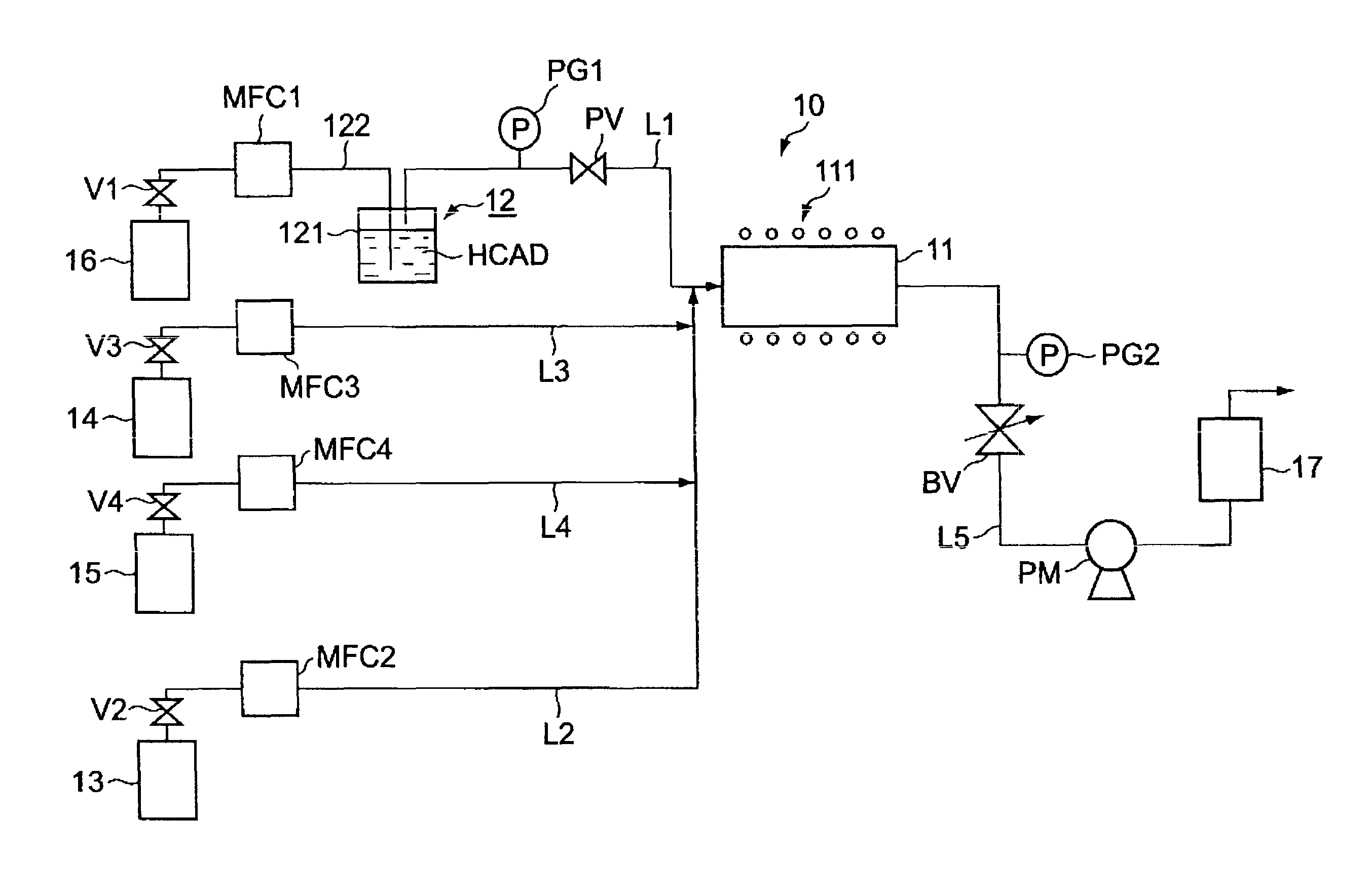
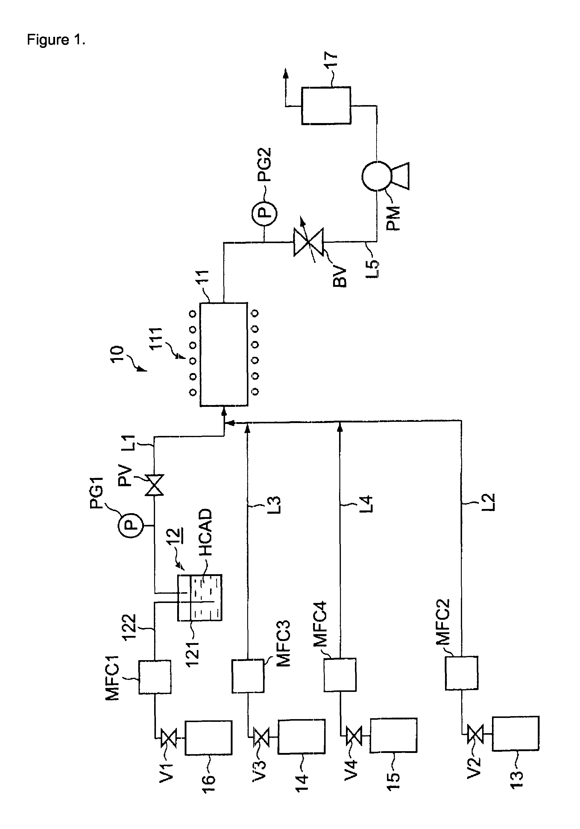
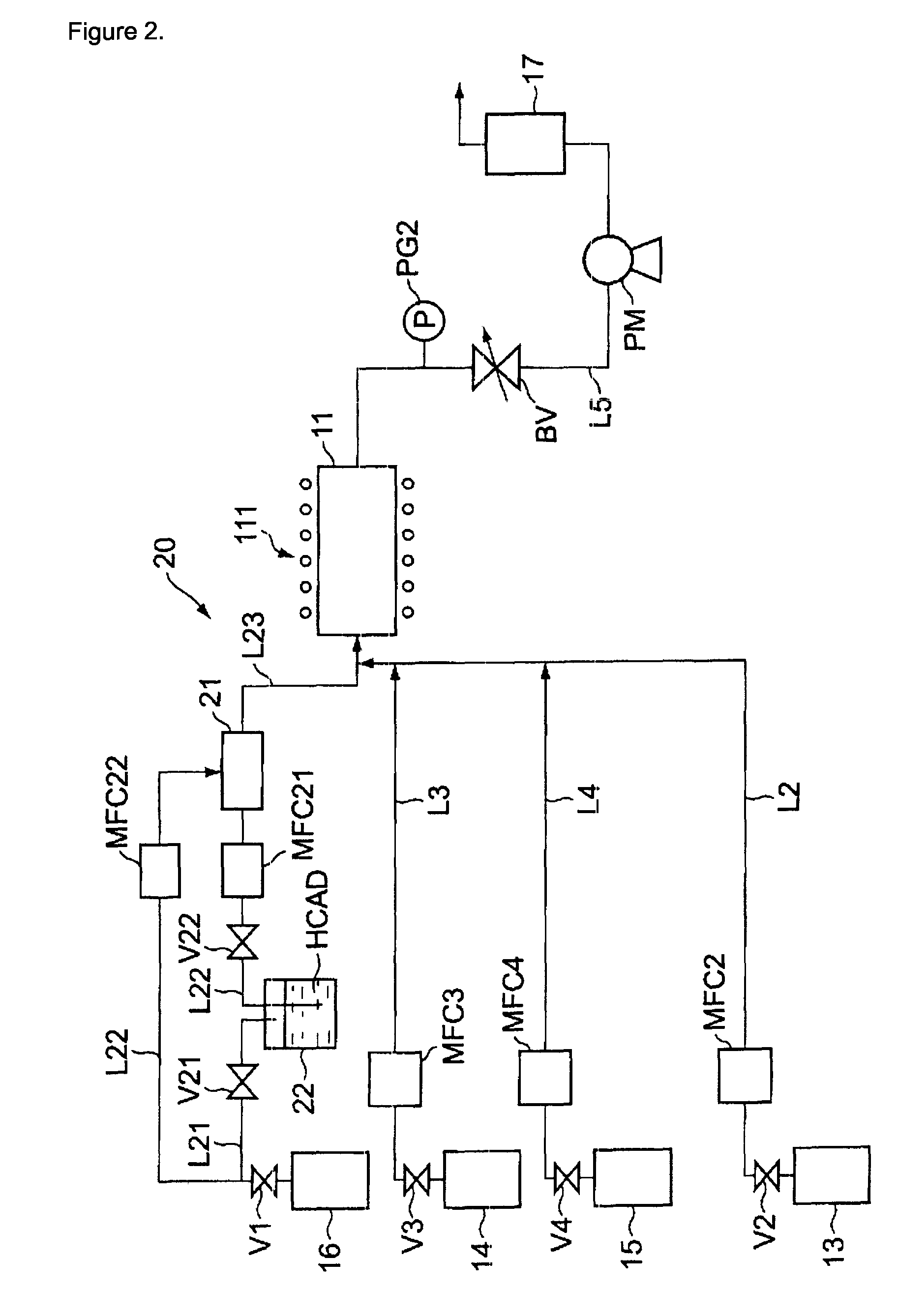
[0059]A typical set-up is described FIG. 1. An inert gas, such as helium, argon, nitrogen or the like having the purity required for semiconductor manufacturing was introduced into the bubbler so that the solution is introduced into the liquid mass flow controller and the vaporizer. The components of the solution are then vaporized at a suitable temperature in order to optimize the delivery. An inert gas, such as helium, argon, nitrogen or the like having the purity required for semi-conductor manufacturing is separately introduced into the vaporizer to carry the gaseous components of the solution to the CVD reactor. It can be mixed with an additional reactant such as ammonia.
[0060]Helium is considered as the most suitable carrier gas in this application.
PUM
| Property | Measurement | Unit |
|---|---|---|
| temperature | aaaaa | aaaaa |
| pressure | aaaaa | aaaaa |
| temperature | aaaaa | aaaaa |
Abstract
Description
Claims
Application Information