Method for fabricating light emitting diode

a technology of light-emitting diodes and manufacturing methods, which is applied in the direction of electrical devices, semiconductor devices, material nanotechnology, etc., can solve the problems of high manufacturing cost and complex manufacturing process

Active Publication Date: 2010-09-02
TSINGHUA UNIV +1
View PDF10 Cites 38 Cited by
  • Summary
  • Abstract
  • Description
  • Claims
  • Application Information

AI Technical Summary

Problems solved by technology

In the above method, the ITO layer is formed on the transparent contact layer via sputtering, and then is to etched to roughen the top surface thereof, which results in a complex manufacturing process and a high manufacturing cost.

Method used


Image

  • Method for fabricating light emitting diode
  • Method for fabricating light emitting diode
  • Method for fabricating light emitting diode

Examples


Embodiment Construction

[0012]The disclosure is illustrated by way of example and not by way of limitation in the figures of the accompanying drawings in which like references indicate similar elements. It should be noted that references to “an” or “one” embodiment in this disclosure are not necessarily to the same embodiment, and such references mean at least one.

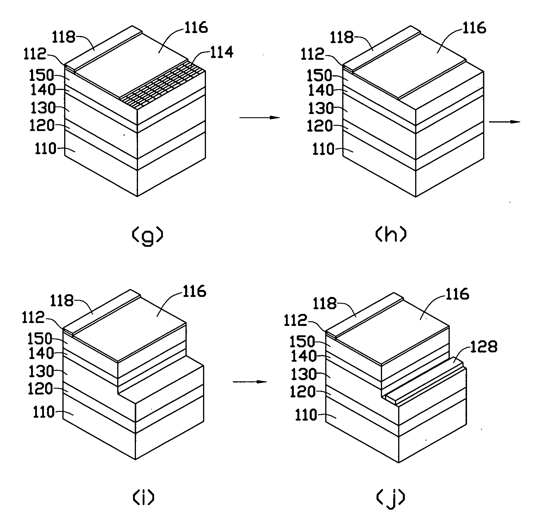
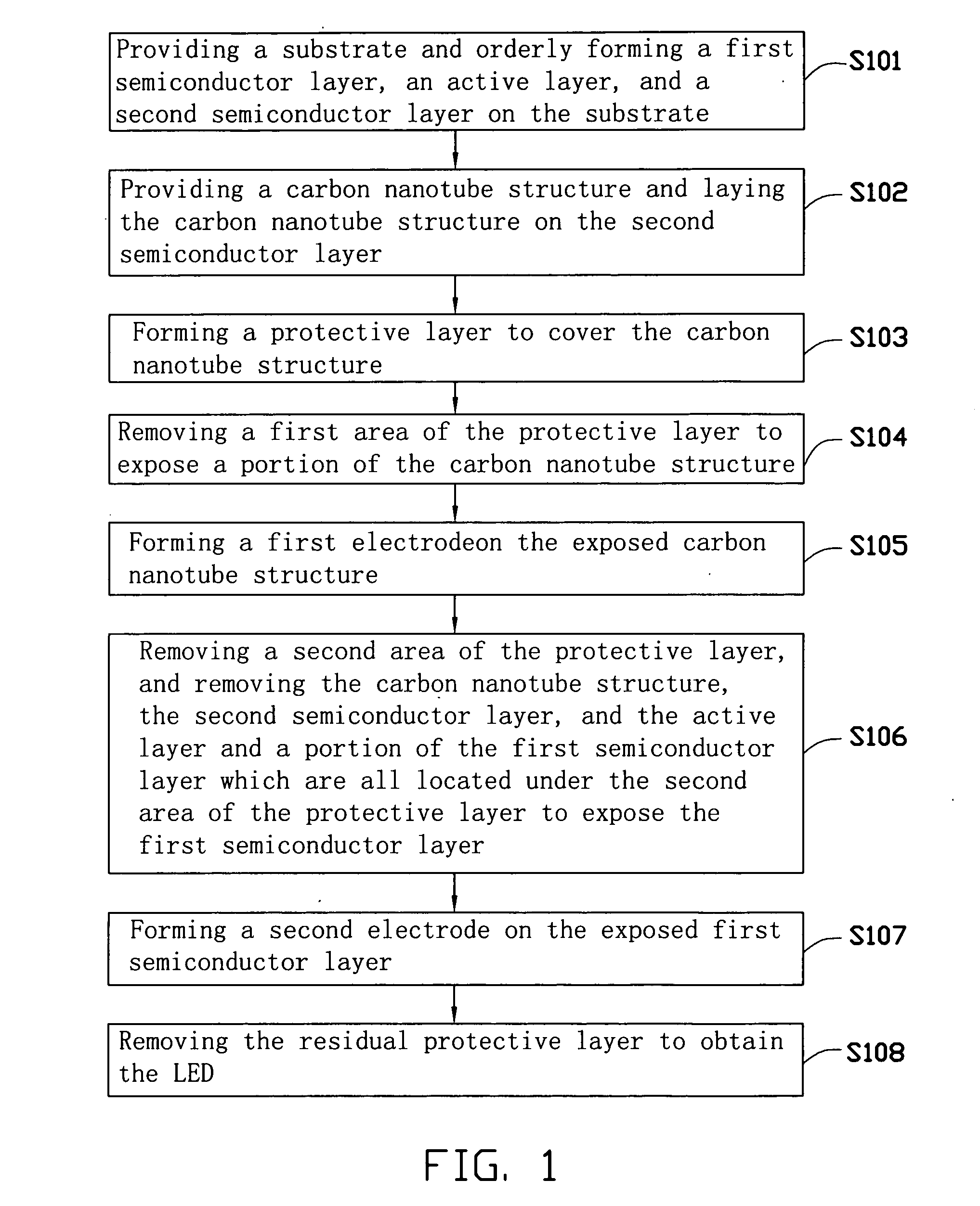
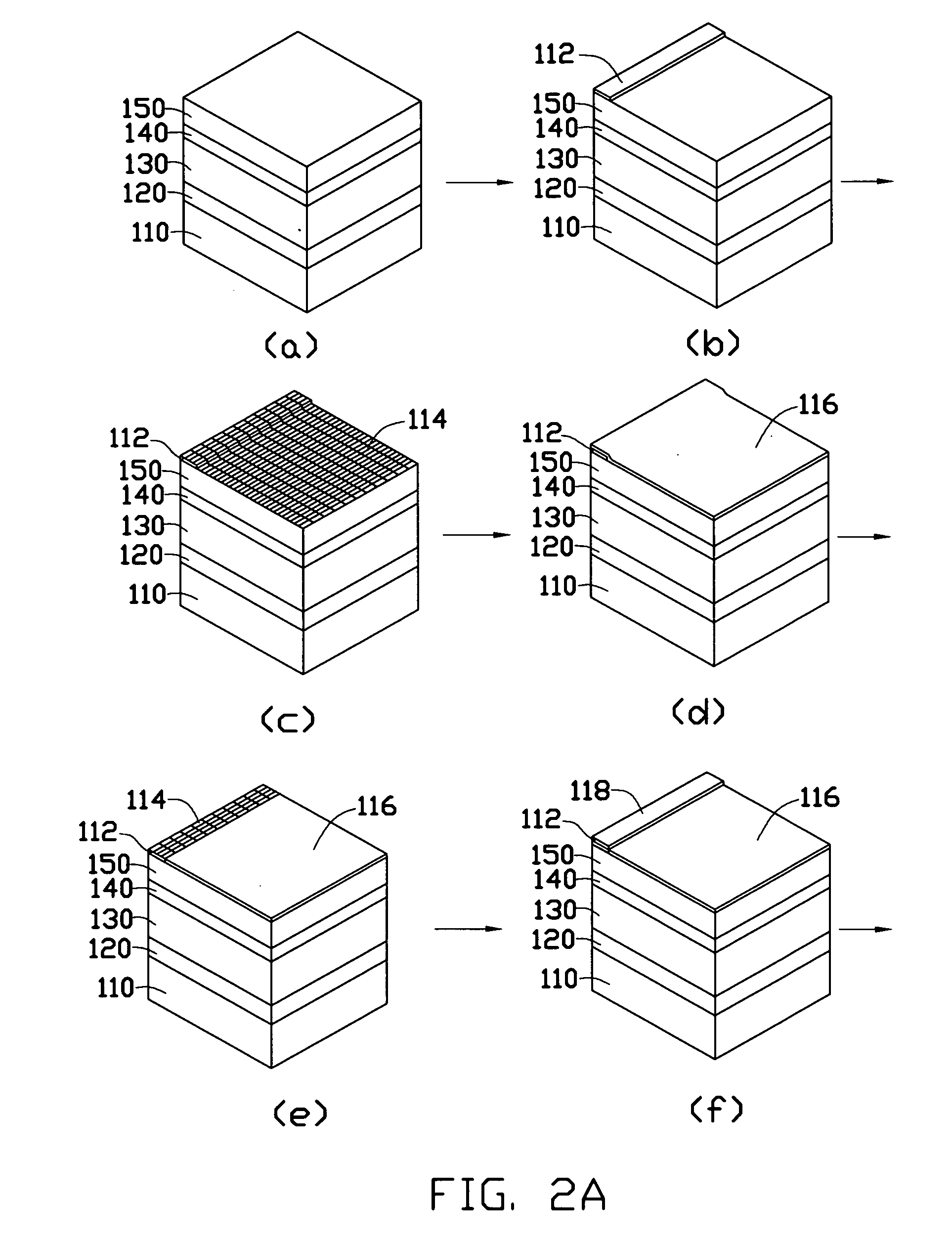
[0013]Referring to FIG. 1 and FIGS. 2A-2B, an embodiment of a method for manufacturing an LED includes the following steps:

[0014]step S101: providing a substrate 110 and orderly forming a first semiconductor layer 130, an active layer 140, and a second semiconductor layer 150 on the substrate 110;

[0015]step S102: providing a carbon nanotube structure 114 and laying the carbon nanotube structure 114 on the second semiconductor layer 150;

[0016]step S103: applying a protective layer 116 to cover the carbon nanotube structure 114;

[0017]step S104: removing a first area of the protective layer 116 to expose a portion of the carbon nanotube structure 11...


PUM

PropertyMeasurementUnit
temperatureaaaaaaaaaa
angleaaaaaaaaaa
thicknessaaaaaaaaaa

Abstract

A method of fabricating a light emitting diode includes the following steps. A substrate is provided and a first semiconductor layer, an active layer, and a second semiconductor layer are placed on the substrate. A carbon nanotube structure is provided and the carbon nanotube structure is lie on the second semiconductor layer. A first electrode is formed on the carbon nanotube structure. A portion of the first semiconductor layer is exposed and a second electrode is formed on the exposed portion of the first semiconductor layer to obtain the light emitting diode.

Description

RELATED APPLICATIONS[0001]This application is related to applications entitled, “LIGHT EMITTING DIODE”, filed______(Atty. Docket No. US23024).BACKGROUND[0002]1. Technical Field[0003]The present disclosure relates to a method for fabricating a light emitting diode (LED).[0004]2. Description of the Related Art[0005]LEDs are semiconductors that convert electrical energy into light. Compared to conventional light sources, the LEDs have higher energy conversion efficiency, higher radiance (i.e., they emit a larger quantity of light per unit area), longer lifetime, higher response speed, and better reliability. At the same time, LEDs generate less heat. Therefore, LED modules are widely used as light sources in optical imaging systems, such as displays, projectors, and so on.[0006]A conventional method of fabricating the LEDs includes the following steps. A GaN bumper layer, a GaN layer, an N-type GaN layer, an active layer and a P-type GaN layer are deposited on a substrate. The active l...

Claims


Application Information

Patent Timeline
Patent Type & Authority Applications(United States)
IPC IPC(8): H01L21/28
CPCB82Y20/00Y10S977/742H01L33/40B82Y30/00
Inventor LI, QUN-QINGJIANG, KAI-LIFAN, SHOU-SHAN
Owner TSINGHUA UNIV
Why Eureka
Try Eureka