Electrical Device with Improved Electrode Surface
- Summary
- Abstract
- Description
- Claims
- Application Information
AI Technical Summary
Benefits of technology
Problems solved by technology
Method used
Image

Examples
example 1
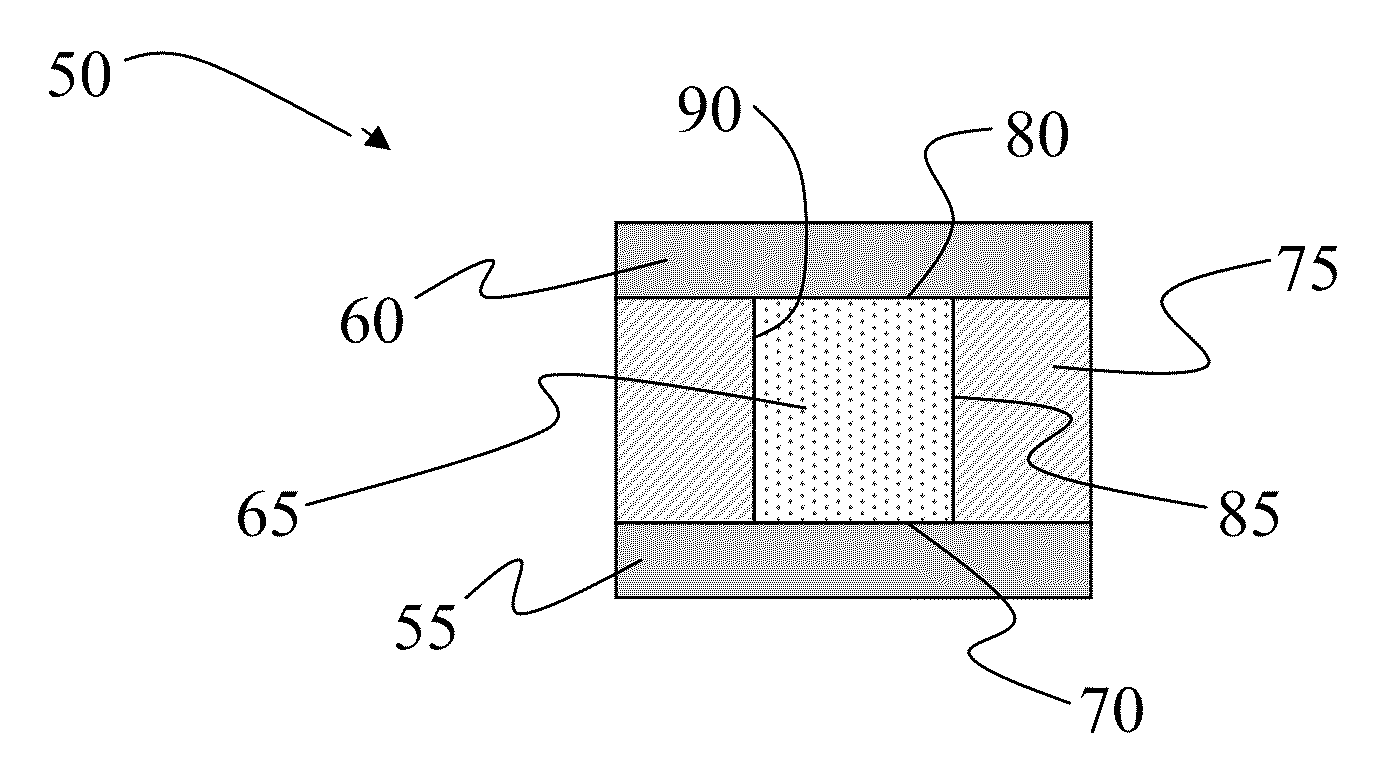
[0089]In this example, the effect of surface treatment on the morphology and surface roughness of an electrode material in a partially fabricated pore device structure is described. FIG. 9A shows a cross-sectional (FIB) image of a pore device at an intermediate stage of fabrication. The device included substrate 305, conductive layer 310 of TiAlN, and dielectric material 315. Conductive layer 310 was formed by sputtering and was not treated before deposition of dielectric material 315 (SiO2). Dielectric material 315 included opening 320, formed by lithography, which exposed portion 325 of the surface of untreated conductive layer 310. Opening 320 had sloped sidewalls and a diameter that varied with depth. The diameter of opening 320 was approximately 72 nm at exposed surface 325 and 146 nm closer to the top surface of dielectric material 315. The structure did not include an active material. Fine-grained Pt layer 330 and large-grained Pt layer 335 were provided as capping layers to ...
example 2
[0095]In this example, the beneficial effect of treating an electrode surface on the electrical properties of an active material device is demonstrated. The device used in this example was large-diameter pore device 500 shown in FIG. 11. Device 500 included substrate 505 having an oxide surface 510. A composite lower electrode was formed on oxide surface 510. The composite lower electrode included conductive TiN layer 515 and conductive carbon layer 520. Dielectric (oxide) material 525 was formed on carbon layer 520 and opening 530 was formed in dielectric material 525. The diameter of opening 530 was approximately 890 nm. Opening 530 exposed a portion 535 of the surface of carbon layer 520. Active material 540 was formed over dielectric material 525 and exposed surface 535. Active material 540 was a phase-change alloy denominated “3405” and had the composition Ge18Sb32Te50. Composite upper electrode 545 was formed over active material 540. Composite upper electrode 545 included a 2...
PUM
 Abstract
Description
Claims
Application Information
 - Generate Ideas
- Intellectual Property
- Life Sciences
- Materials
- Tech Scout
- Unparalleled Data Quality
- Higher Quality Content
- 60% Fewer Hallucinations
Browse by: Latest US Patents, China's latest patents, Technical Efficacy Thesaurus, Application Domain, Technology Topic, Popular Technical Reports.
© 2025 PatSnap. All rights reserved.Legal|Privacy policy|Modern Slavery Act Transparency Statement|Sitemap|About US| Contact US: help@patsnap.com