Interface Techniques for Coupling a Microchannel Plate to a Readout Circuit

a readout circuit and microchannel plate technology, applied in the field of sensors, can solve the problems of reducing detection efficiency, reliability, cost, weight and power, and difficulty in fabricating a roic that is compatible with such large sized active areas, and achieves good thermal match and denser pixel resolution

Active Publication Date: 2010-09-09
BAE SYST INFORMATION & ELECTRONICS SYST INTERGRATION INC
View PDF2 Cites 5 Cited by
  • Summary
  • Abstract
  • Description
  • Claims
  • Application Information

AI Technical Summary

Benefits of technology

[0009]One embodiment of the present invention provides a readout reducer device for interfacing a multi-channel sensor with a readout integrated circuit (ROIC). The device includes an array of anode pads, each anode pad for receiving a detection signal from a corresponding channel of the sensor. The device further includes a ROIC interconnect having an array of ROIC pads that couples to a corresponding array of the ROIC. The device further includes at least one interconnect layer for physically connecting each anode pad to a corresponding one of the ROIC pads. The array of anode pads is a different size than that array of ROIC pads (in one such case, the array of anode pads is larger than the array of ROIC pads). The sensor can be, for example, a microchannel plate (MCP). Other suitable multi-channel sensors include, for instance, an array of photodiodes selected from materials that respond to photons in a band of interest (e.g., UV to IR), or an array of avalanche photodiodes responsive to the band of interest. In one particular case, the device includes first and second interconnect layers, wherein the first interconnect layer physically connects some of the anode pads to their respective ROIC pads, and the second interconnect layer physically connects others of the anode pads to their respective ROIC pads. The at least one interconnect layer can be formed

Problems solved by technology

A problem associated with conventional MCP-based detectors is that MCPs typically have large active areas (active areas of 18 and 25 mm in diameter are standard), which are useful in collecting signal, but require a correspondingly large sized readout integrated circuit (ROIC).
In short, it is difficult and expensive to fabricate a ROIC that is compatible with such large sized MCP active areas.
Howeve

Method used


Image

  • Interface Techniques for Coupling a Microchannel Plate to a Readout Circuit
  • Interface Techniques for Coupling a Microchannel Plate to a Readout Circuit
  • Interface Techniques for Coupling a Microchannel Plate to a Readout Circuit

Examples


Embodiment Construction

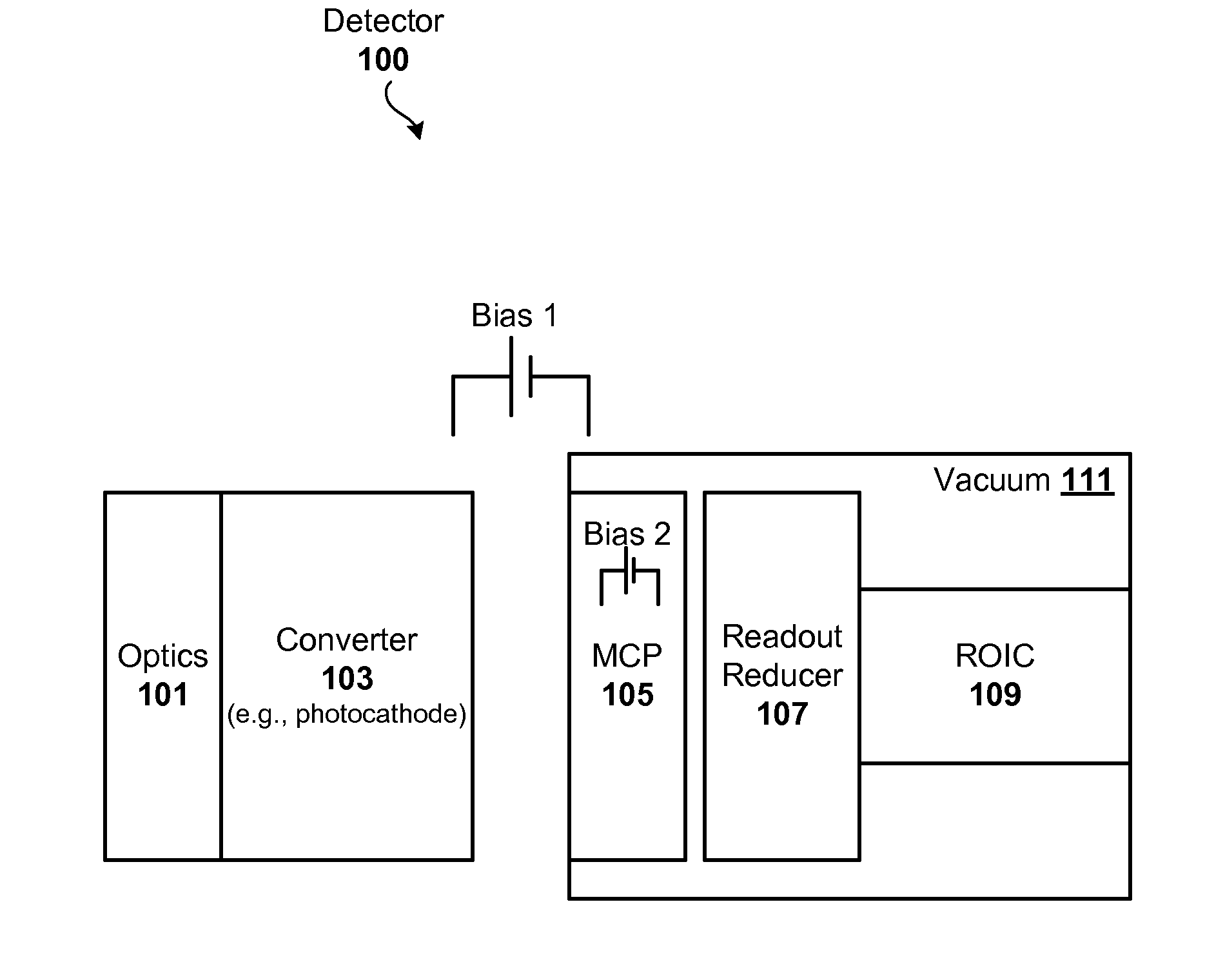
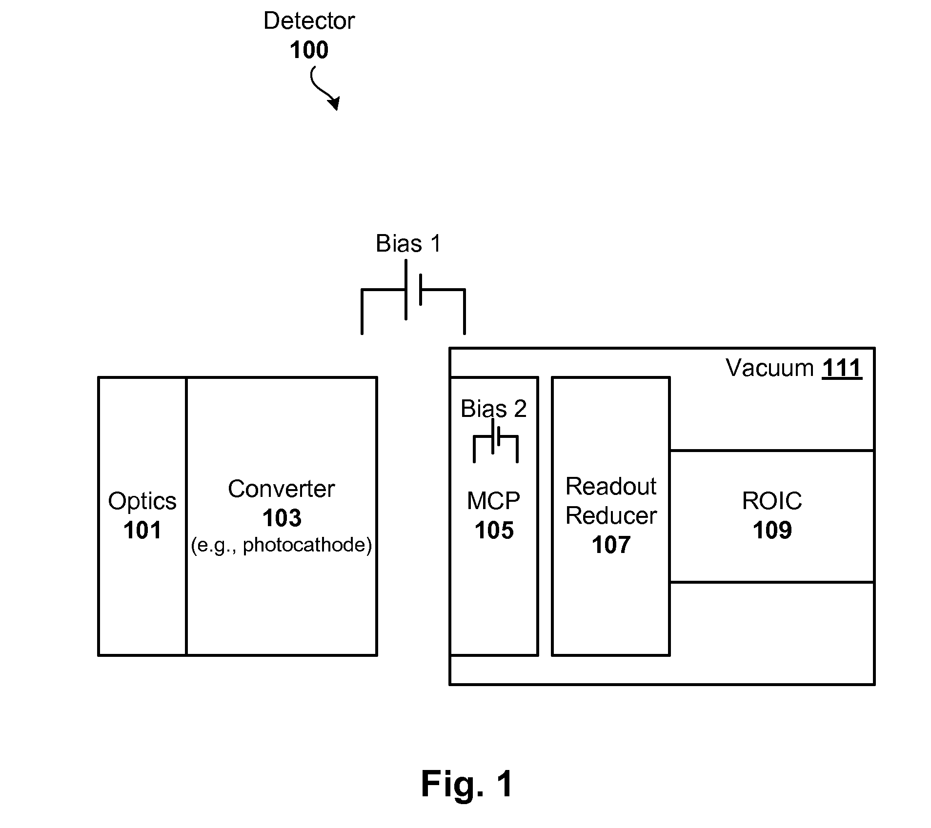
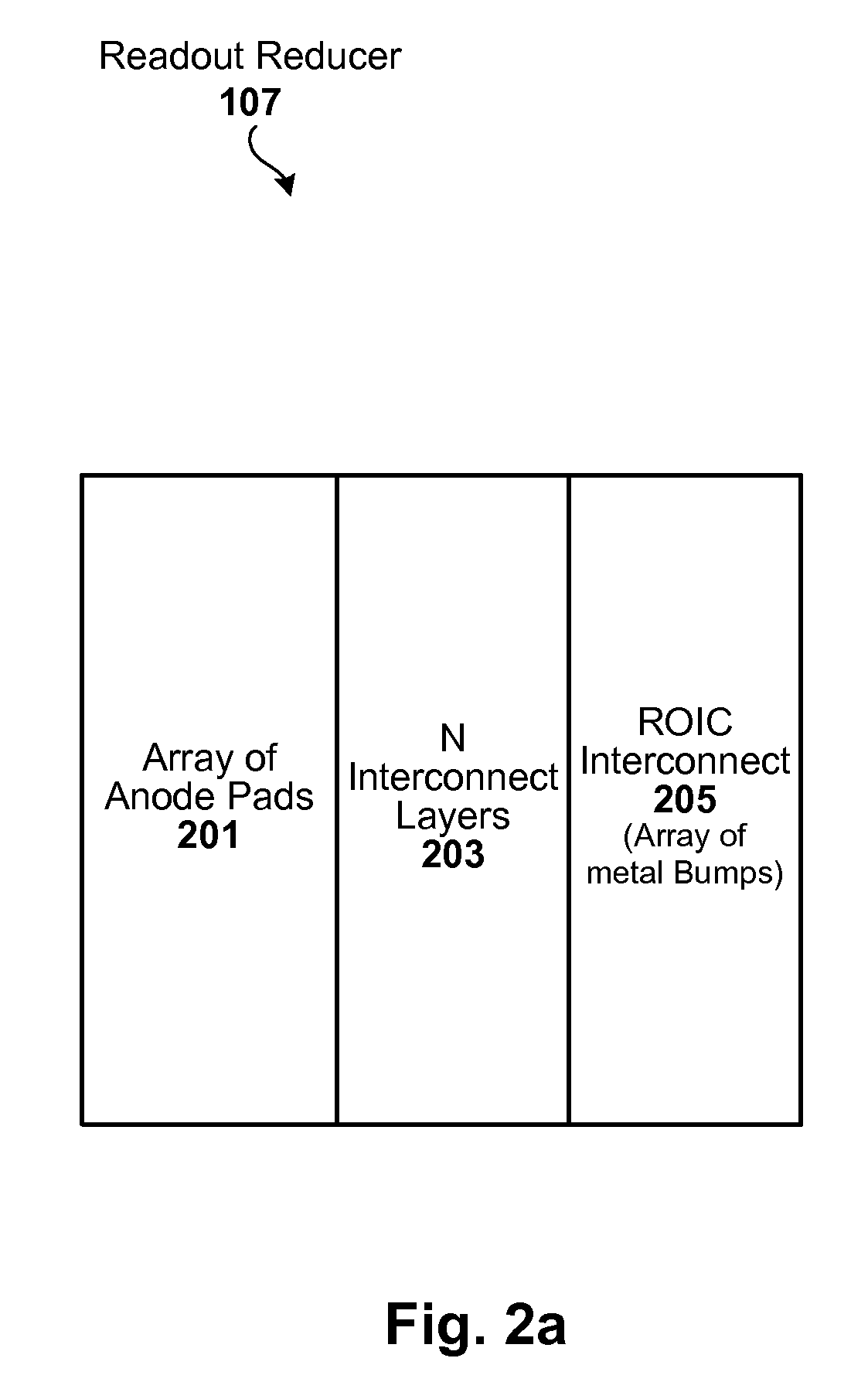
[0021]Techniques are disclosed that can be used to interface a microchannel plate (MCP) with readout circuitry. The techniques can be employed, for instance, with MCP based devices used in a numerous sensing / detection applications, and are particularly suitable for applications where it is desirable to interface an MCP having a relatively large active area to a readout circuit having a relatively smaller active area. The interface can be carried out on a pixel-to-pixel basis and effectively reduces a relatively large MCP image to a smaller ROIC image. The interface may also be configured with flexible anode pad geometry, which allows for compensation of optical blur variations and very high fill factor. The interface can be made using standard semiconductor materials and photolithography techniques, and can be configured with thermal expansion qualities that closely track or otherwise match that of the readout circuitry.

[0022]General Overview

[0023]As previously explained, MCP sensor...


PUM


Abstract

Techniques are disclosed that can be used to interface a microchannel plate (MCP) with readout circuitry. The techniques can be employed, for instance, with MCP based devices used in a numerous sensing/detection applications, and are particularly suitable for applications where it is desirable to interface an MCP having a relatively large active area to a readout circuit having a relatively smaller active area. The interface effectively decouples anode geometry from ROIC geometry and may also be configured with flexible anode pad geometry, which allows for compensation of optical blur variations as well as a very high fill factor. The interface can be made using standard semiconductor materials and photolithography techniques, and can be configured with thermal expansion qualities that closely track or otherwise match that of the readout circuitry.

Description

RELATED APPLICATIONS[0001]This application is related to U.S. application Ser. No. ______ (Attorney Docket BAE20070078), filed Mar. 9, 2009, and titled “Selective Channel Charging for Microchannel Plate” which is herein incorporated by reference in its entirety.FIELD OF THE INVENTION[0002]The invention relates to sensors such as microchannel plates (MCPs), and more particularly, to techniques for interfacing sensors to readout circuitry.BACKGROUND OF THE INVENTION[0003]As is known, a microchannel plate (MCP) includes an array of small diameter tubes or channels, each of which operates as an independent electron multiplier in the presence of an electric field applied to the MCP. As a signal (e.g., an electron, photon, ion) enters the input end of a given channel and passes through that channel, it impacts the channel walls thereby producing so-called secondary electrons that then also propagate through the channel and impact the channel wall to produce even more secondary electrons. ...

Claims


Application Information

Patent Timeline
IPC IPC(8): H01J40/14H01J43/00
CPCH01J31/507H01L27/14609H01J43/246H01J43/12
Inventor DEFLUMERE, MICHAEL E.SCHOECK, PAUL W.
Owner BAE SYST INFORMATION & ELECTRONICS SYST INTERGRATION INC
Why Eureka
Try Eureka