

Solid state image pickup device, method of manufacturing the same, image pickup device, and electronic device
- Summary
- Abstract
- Description
- Claims
- Application Information
AI Technical Summary
Benefits of technology
Problems solved by technology
Method used
Image

Examples
first embodiment
1. First Embodiment
[0108]First Exemplary Configuration of Solid State Image Pickup Device
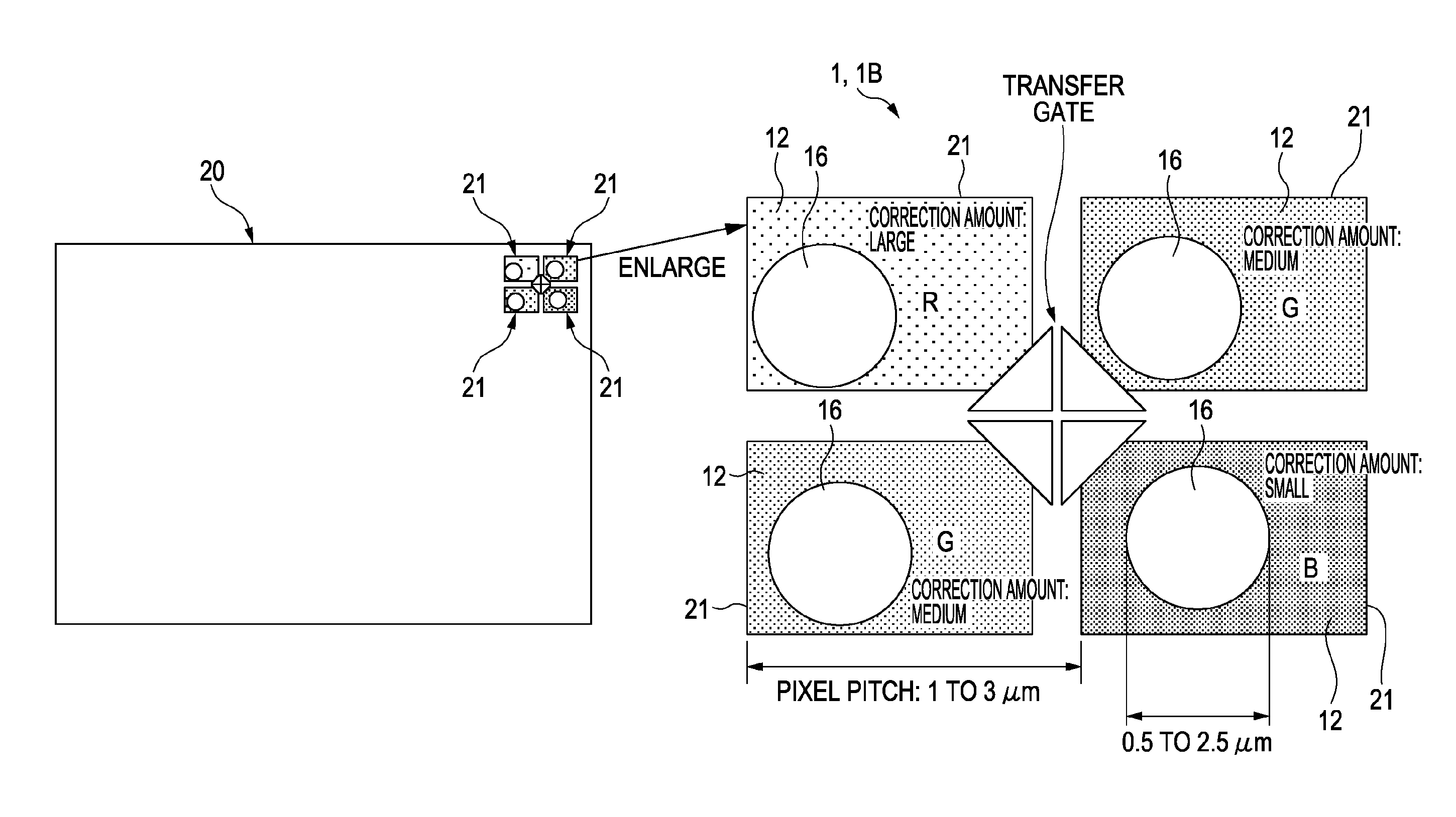
[0109]A first exemplary configuration of a solid state image pickup device according to a first embodiment of the present invention will be described with reference to schematic cross-sectional views and a plan layout diagram in FIGS. 3A to 3C. FIG. 3A illustrates a unit pixel at the center of an angular field, FIG. 3B illustrates a unit pixel at an edge of the angular field, and FIG. 3C illustrates a pixel section including a plurality of unit pixels.
[0110]Hereinafter, reference sign 1 denotes a solid state image pickup device, 11 denotes a semiconductor substrate, 12 denotes a photoelectric transducer, 14 denotes an interlayer insulating film, 16 denotes a waveguide, 17 denotes a color filter layer, 18 denotes a microlens, 19 denotes a waveguide hole, 20 denotes a pixel section, 21 denotes a unit pixel, 53 denotes a waveguide material film, 200 denotes an image pickup device, 201 denotes an im...
second embodiment
2. Second Embodiment
[0191]First Exemplary Method of Manufacturing Solid State Image Pickup Device
[0192]Next, a first exemplary method of manufacturing a solid state image pickup device according to a second embodiment of the present invention will be described with reference to FIGS. 12 to 21.
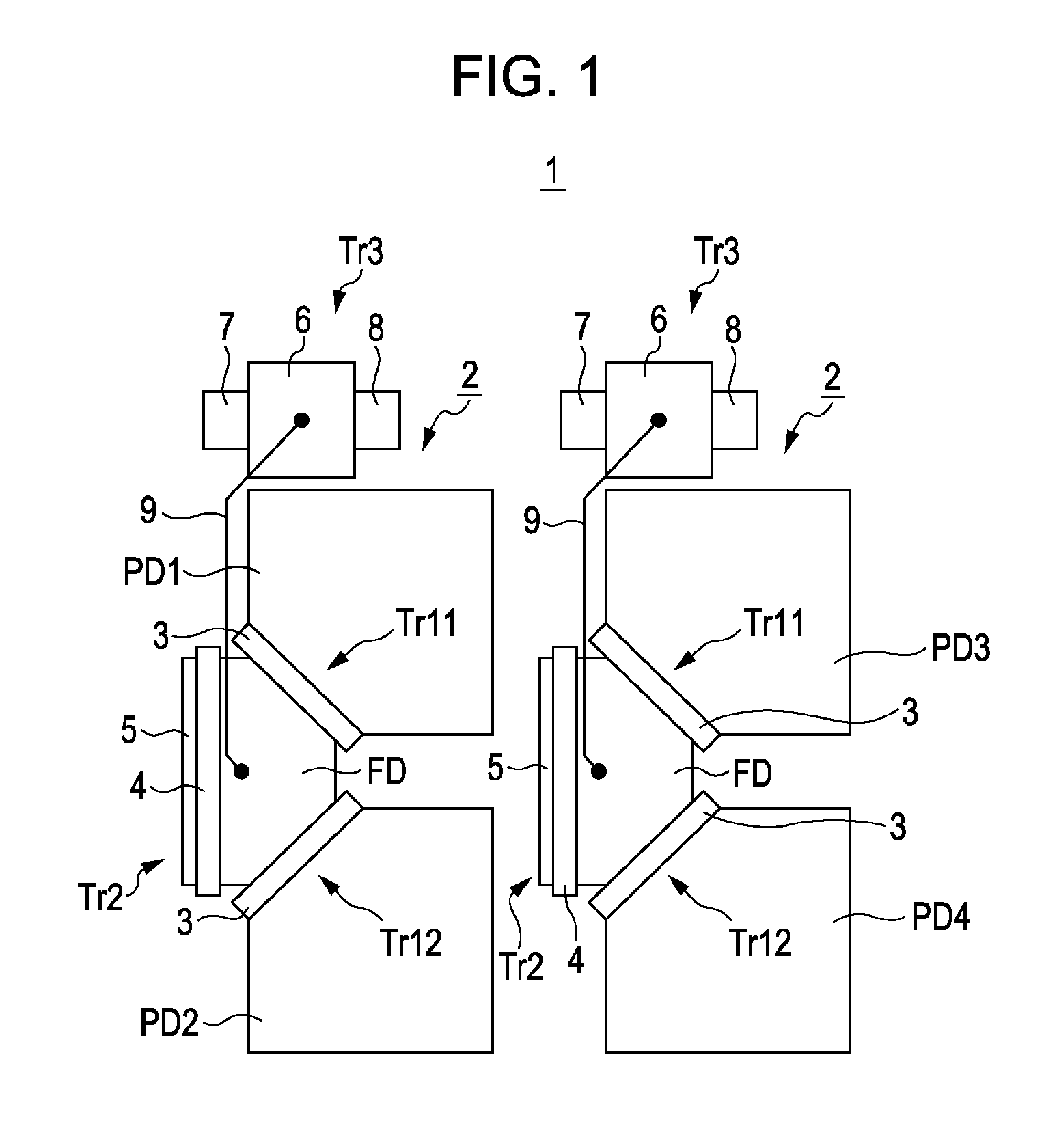
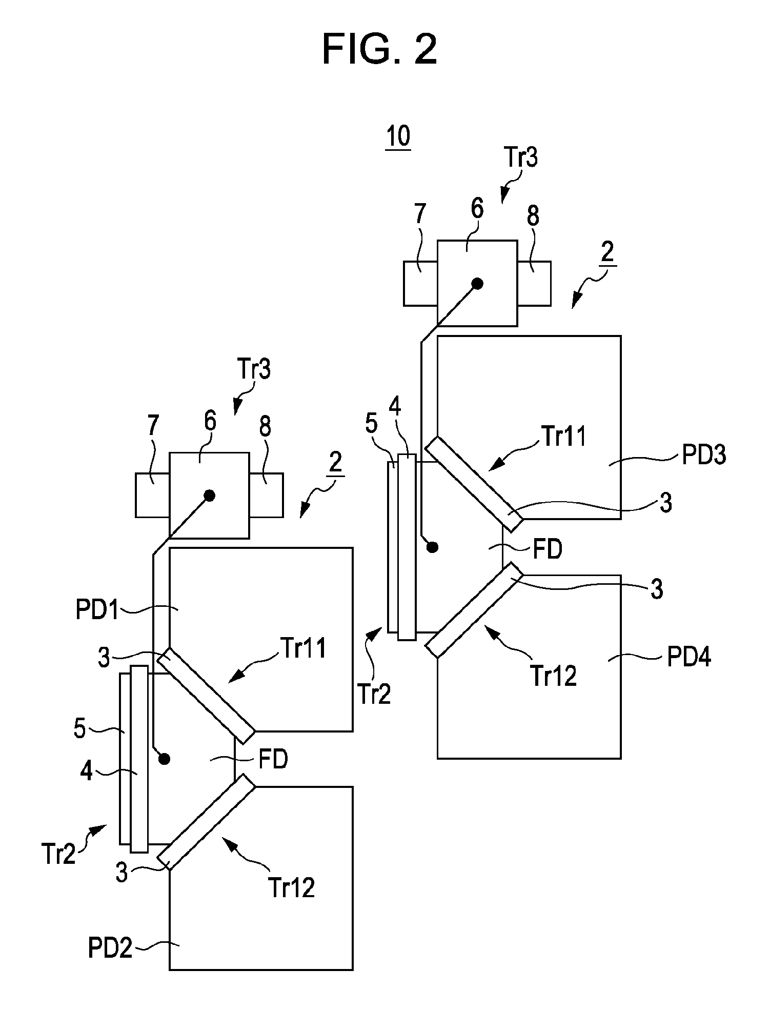
[0193]Referring to FIG. 12, a photoelectric transducer 12 is formed on a surface (light incident side) of a semiconductor substrate 11. The photoelectric transducer 12 converts incident light into a signal charge. Also, a transfer gate 31 is formed on the semiconductor substrate 11. The transfer gate 31 reads the signal charge which has been subjected to the photoelectric transduction by the photoelectric transducer 12. Further, though not shown, a pixel transistor and a peripheral circuit unit are formed on the semiconductor substrate 11. The pixel transistor amplifies and outputs the signal charge which has been subjected to the photoelectric transduction by the photoelectric transducer 12. T...
third embodiment
3. Third Embodiment
[0218]Example Configuration of Image Pickup Device
[0219]Next, an exemplary configuration of an image pickup device according to a third embodiment of the present invention will be described with reference to FIG. 29. This image pickup device uses a solid state image pickup device according to the embodiment of the present invention.
[0220]Referring to FIG. 29, an image pickup device 200 includes an image pickup unit and a solid state image pickup device 210. A light condensing optical unit 202 for forming an image is provided at the light-condensing side of the image pickup unit 201. The image pickup unit 201 is connected to a signal processing unit 203. The signal processing unit 203 includes a drive circuit that drives the image pickup unit 201; and a signal processing circuit that processes a signal, which has been subjected to photoelectric transduction by the solid state image pickup device 210, to be an image. The image signal processed by the signal processi...
PUM
 Abstract
Description
Claims
Application Information