Adhesive sheet for manufacturing semiconductor device, and semiconductor device manufacturing method using the sheet

Inactive Publication Date: 2010-09-23
NITTO DENKO CORP
View PDF3 Cites 11 Cited by
  • Summary
  • Abstract
  • Description
  • Claims
  • Application Information

AI Technical Summary

Benefits of technology

[0021]According to the manufacturing method of the present invention, since an adhesive sheet containing a pigment capable of absorbing or reflecting light having a wavelength in a range from 290 to 450 nm added therein is used, it becomes easy to identify the adhesive sheet upon lamination with a semiconductor wafer or a dicing sheet, and also the lamination accuracy can be improved. As a result, it

Problems solved by technology

However, as thinning and miniaturization of a semiconductor package progress, the adhesive sheet used for the production becomes thinner.
Therefore, it becomes difficult to detect the adhesive sheet using the optical sensor in the respective manufacturing processes.
As a result, for example, when the adhesive sheet is laminated with a dicing sheet, lamination may n

Method used


Image

  • Adhesive sheet for manufacturing semiconductor device, and semiconductor device manufacturing method using the sheet
  • Adhesive sheet for manufacturing semiconductor device, and semiconductor device manufacturing method using the sheet
  • Adhesive sheet for manufacturing semiconductor device, and semiconductor device manufacturing method using the sheet

Examples


example 1

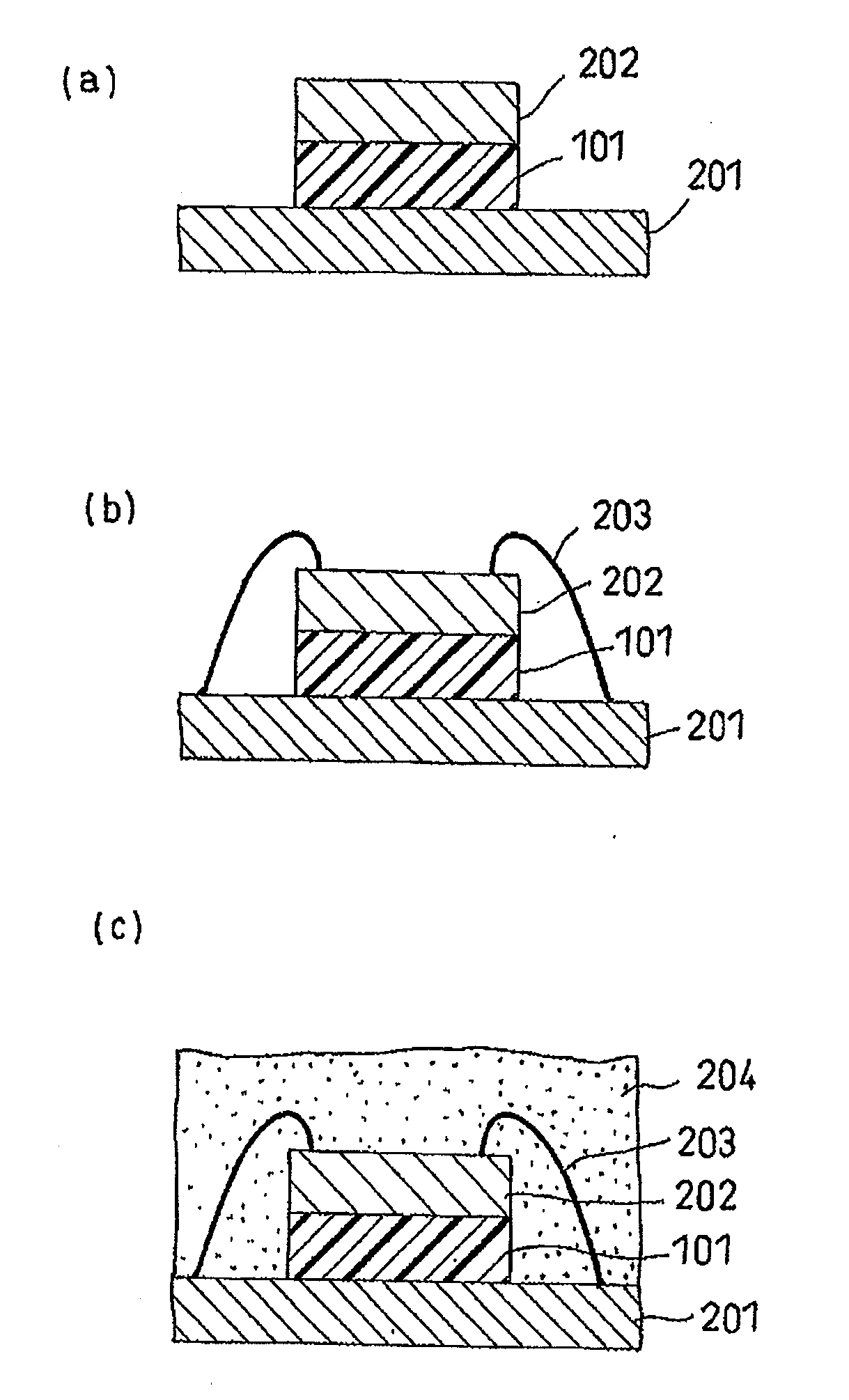
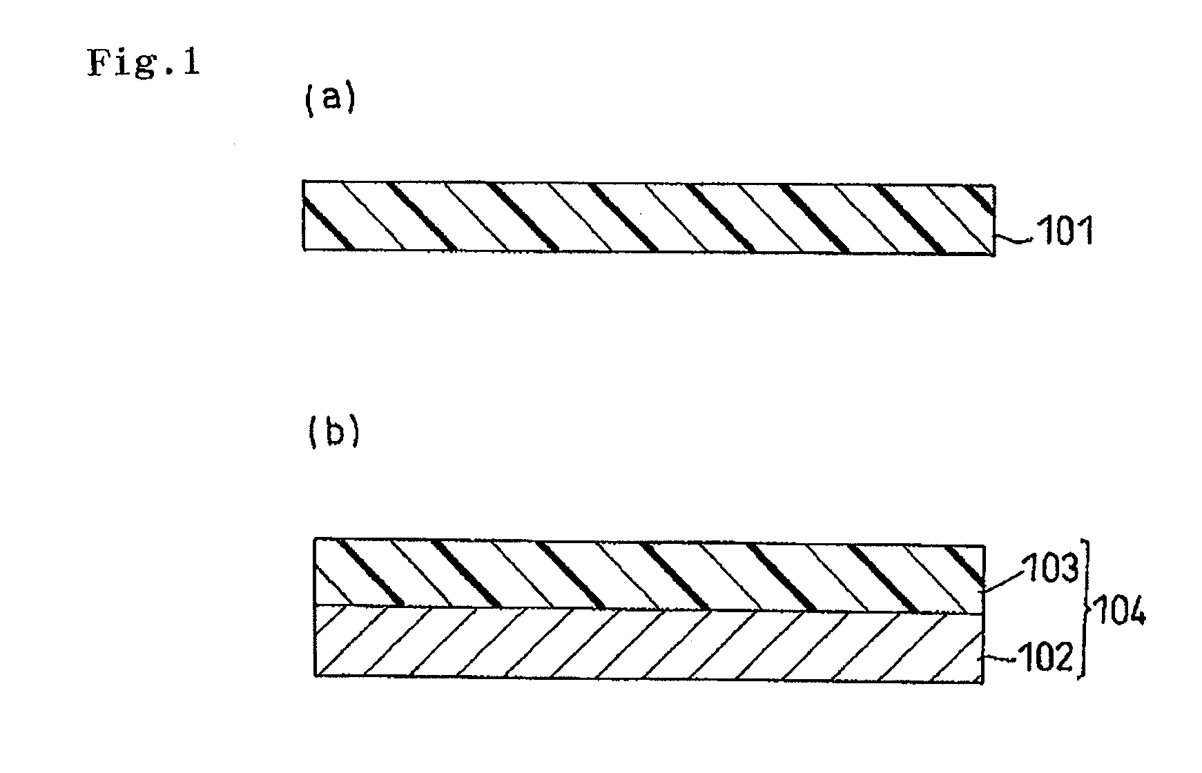
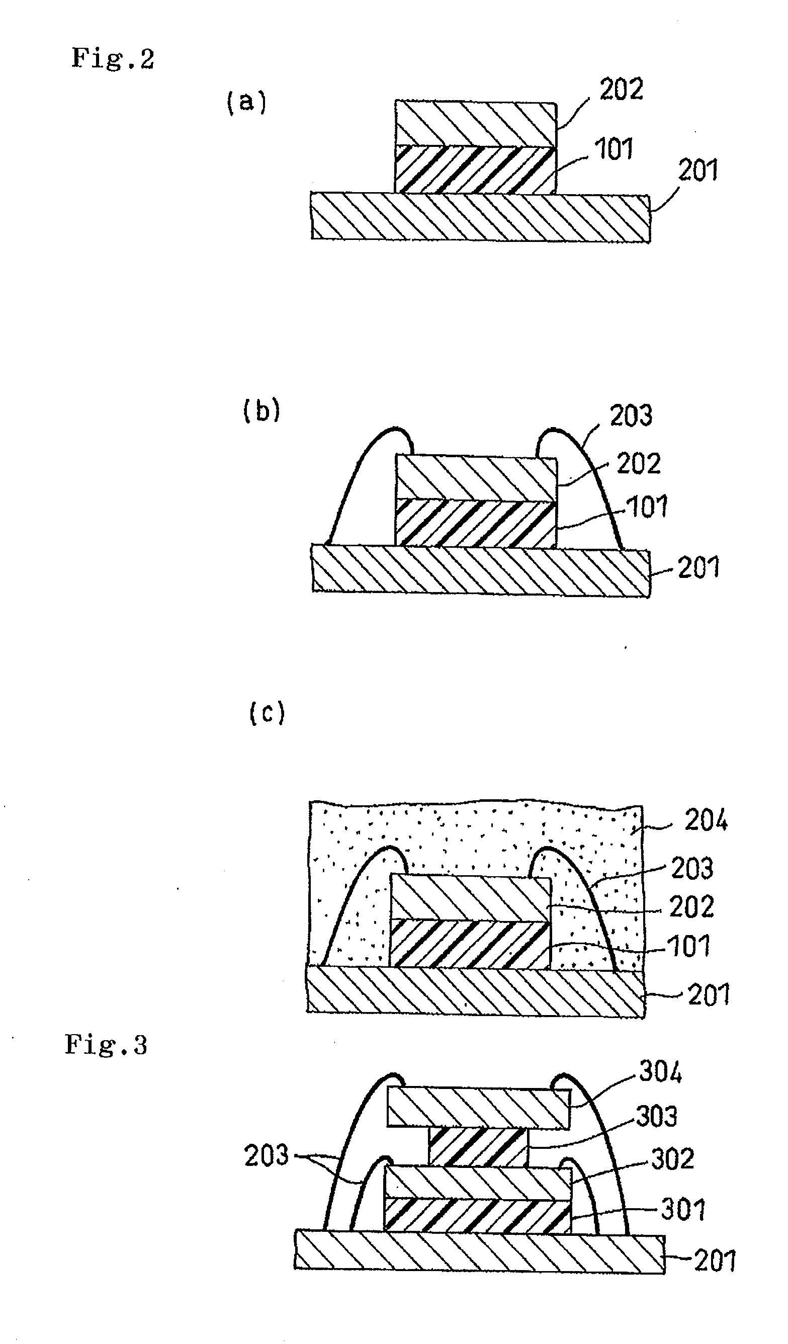
[0089]First, 100 parts of a polymer containing butyl acrylate as a main component (manufactured by Negami Chemical industrial Co., Ltd. under the trade name of PARACRON SN-710), 3 parts of an isocyanate-based crosslinking agent (manufactured by NIPPON POLYURETHANE INDUSTRIES Co., Ltd. under the trade name of Coronate HX), 33 parts of an epoxy resin (manufactured by Japan Epoxy Resins CO., LTD. under the trade name of EPICOAT 1003), 22 parts of a phenol resin (manufactured by ARAKAWA CHEMICAL INDUSTRIES, LTD. under the trade name of P-180) and 0.2 parts of ultrafine titanium oxide particles (manufactured by Titan Kogyo, Ltd. under the trade name of STT-4D, average particle diameter: 0.15 μm) were dissolved in methyl ethyl ketone, followed by stirring to prepare a solution of an adhesive composition (concentration: 15% by weight).

[0090]The adhesive composition solution was kneaded and dispersed by a three-roll mill, centrifuged at 400 ppm and then filtered through a glass filter havin...

example 2

[0092]To 100 parts of an acryl-based adhesive, 3 parts of an isocyanate-based crosslinking agent (manufactured by NIPPON POLYURETHANE INDUSTRIES Co., Ltd. under the trade name of Coronate HX) was added to prepare an acryl-based adhesive composition. The acryl-based adhesive composition was obtained by mixing 70 parts of 2-ethylhexyl acrylate, 25 parts of n-butyl acrylate and 5 parts of acrylic acid to prepare an acryl-based copolymer composed of these monomers, and dissolving the acryl-based copolymer and 1 part of Fastgen blue GNPS (manufactured by Dainippon Ink and Chemicals, Incorporated, blue pigment: copper phthalocyanine-based pigment, average particle diameter: 0.1 μm) in methyl ethyl ketone in a concentration of 15%.

[0093]In the same manner as in Example 1, centrifugation was performed and then filtration was performed to manufacture an adhesive sheet comprising a mold-release treated film and an adhesive layer having a thickness of 7 μm laminated on the mold-release treated...


PUM

PropertyMeasurementUnit
Temperatureaaaaaaaaaa
Pressureaaaaaaaaaa

Abstract

The present invention provides an adhesive sheet for manufacturing a semiconductor device, which, even when the adhesive sheet is made thin, makes it possible to easily identify the presence or absence of the adhesive sheet, thereby decreasing down time for the manufacturing apparatus and enabling an improvement of the yield, and to provide a semiconductor device manufacturing method using the sheet. The present invention relates to an adhesive sheet for manufacturing a semiconductor device which is used to adhere a semiconductor element to an adherend, wherein the adhesive sheet contains a pigment which adsorbs or reflects light having a wavelength in a range from 290 to 450 nm.

Description

TECHNICAL FIELD[0001]The present invention relates to an adhesive sheet for manufacturing a semiconductor device which is used when a semiconductor element is adhered to an adherend such as a lead frame, a TAB film, a substrate, or a separately manufactured semiconductor chip, followed by wire-bonding to the semiconductor device, and to a semiconductor device manufacturing method using the sheet.BACKGROUND ART[0002]In a conventional method for manufacturing a semiconductor device, a semiconductor wafer with a pattern formed thereon is diced on each semiconductor chip and then die-bonded on a substrate, a lead frame or other semiconductor chips using a thermal curable paste resin (for example, Patent Document 1 described below). After wire-bonding to semiconductor chips, the semiconductor chips are sealed with a sealing resin to manufacture a semiconductor package.[0003]Also, use of an adhesive sheet using a thermal curable resin and a thermoplastic resin in combination in place of t...

Claims


Application Information

Patent Timeline
IPC IPC(8): C09J7/00B32B37/12C09J7/35
CPCC09J7/0203C09J7/0217C09J11/04C09J133/08H01L23/24H01L23/3121H01L24/83H01L2224/32145H01L2224/32225H01L2224/48091H01L2224/48227H01L2224/73265H01L2224/92247H01L2924/01004H01L2924/01013H01L2924/0102H01L2924/01025H01L2924/01029H01L2924/0103H01L2924/01033H01L2924/01046H01L2924/01047H01L2924/01051H01L2924/01056H01L2924/01057H01L2924/01077H01L2924/01079H01L2924/01082H01L24/29H01L24/48H01L2224/2919H01L2924/01005H01L2924/01006H01L2924/01019H01L2924/01024H01L2924/01045H01L2924/0105H01L2924/014H01L2924/0665H01L2224/45124H01L2224/45144H01L2224/45147H01L24/45H01L2224/83H01L2924/01015Y10T156/10H01L2924/00014H01L2924/00012H01L2924/00H01L2924/3512H01L2924/15747H01L2924/15788H01L2924/181H01L24/73C09J7/35C09J7/385Y10T428/249921
Inventor AMANO, YASUHIROMISUMI, SADAHITOMATSUMURA, TAKESHITAKAMOTO, NAOHIDE
Owner NITTO DENKO CORP
Why Eureka
Try Eureka