Method of manufacturing a semiconductor device

a manufacturing method and semiconductor technology, applied in the direction of semiconductor devices, electrical appliances, transistors, etc., can solve the problems of reducing the oxidation rate of reducing agents, so as to avoid the variation of characteristics of semiconductor devices. , the effect of increasing the rate of oxidation reaction

Active Publication Date: 2010-09-23
FUJI ELECTRIC CO LTD
View PDF9 Cites 25 Cited by
  • Summary
  • Abstract
  • Description
  • Claims
  • Application Information

AI Technical Summary

Benefits of technology

[0048]In the inventions described above, the second metal film, which is the outermost surface of the front surface electrode, is formed with a main component of nickel, which enhances the rate of oxidation reaction of the reducing agent added to the plating bath. In addition, the surface of the front surface electrode is activated before the electroless plating process. Owing to these measures, the first plated film is continuously precipitated on the surface of the second metal film in the electroless plating process solely by an oxidation-reduction reaction between the second metal film and the reducing agent. Consequently, the procedure of the invention precludes the need in the convent

Problems solved by technology

In addition, the PT type IGBT is relatively expensive because of the use of an epitaxial substrate.
In the electroless plating process on the front surface electrode, the surface of the front surface electrode needs to be activated to enhance adhesiveness between the front surface electrode and the plated fil

Method used


Image

  • Method of manufacturing a semiconductor device
  • Method of manufacturing a semiconductor device
  • Method of manufacturing a semiconductor device

Examples


Embodiment Construction

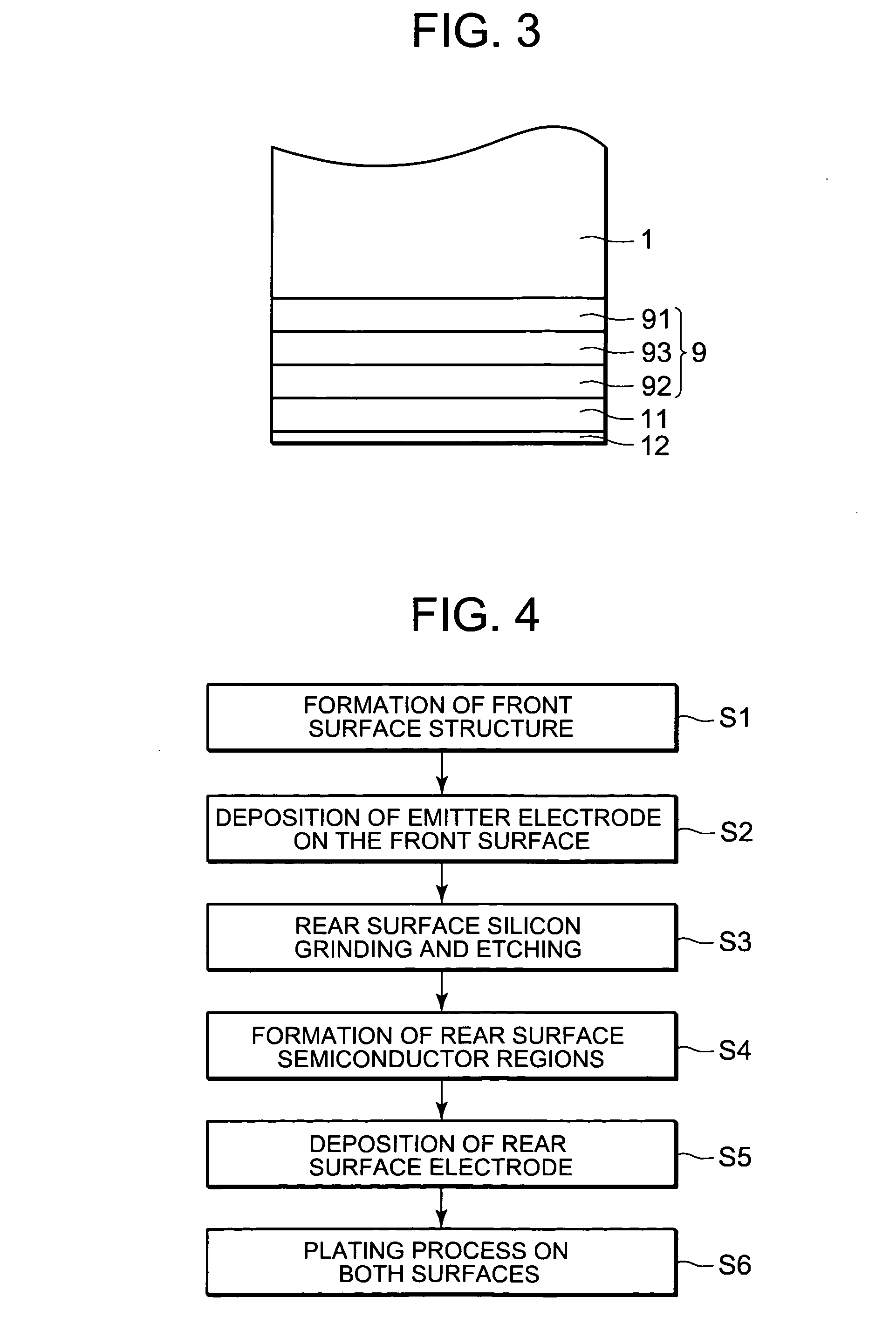
[0065]Now, some preferred embodiment examples of a method of manufacturing a semiconductor device according to the present invention and semiconductor devices manufactured by the method will be described in detail in the following with reference to the accompanying drawings. Throughout the description on all the embodiment examples and in all the accompanying drawings, the similar structures are given the same symbols and repeated description thereon is avoided.

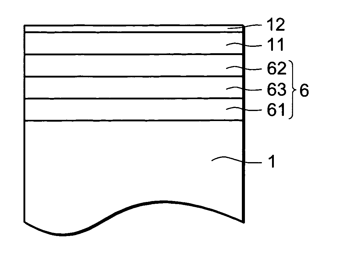
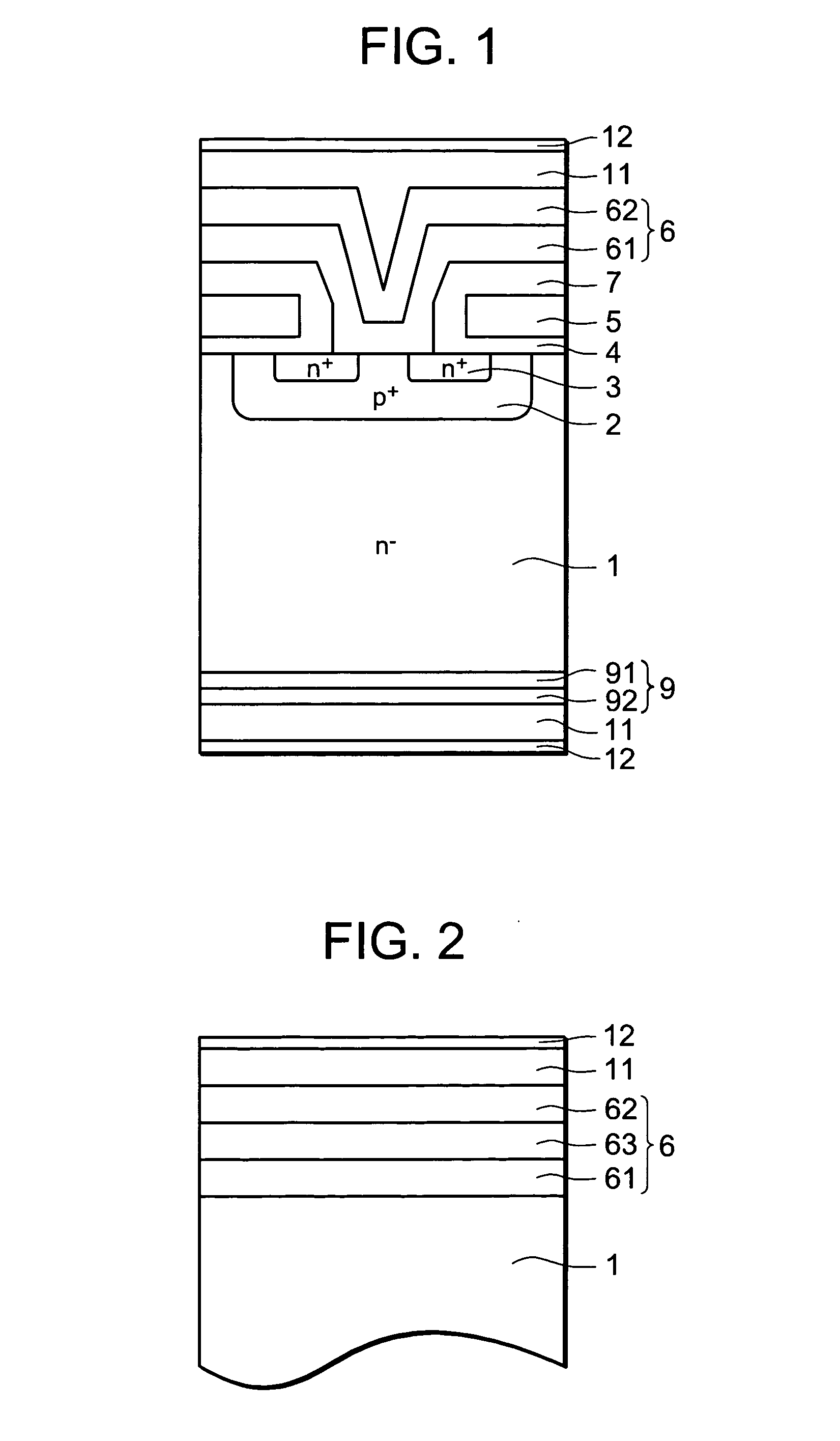
[0066]FIG. 1 is a sectional view showing a semiconductor device manufactured by an embodiment of a method of manufacturing a semiconductor device according to the invention. Referring to FIG. 1, a p+ base region 2 is provided in a portion of a front surface layer of a semiconductor substrate 1 in the front surface side of the semiconductor device. An n+ emitter region 3 is selectively provided in a portion of the surface layer of the p+ base region 2. A gate electrode 5 is provided on a portion of the semiconductor substrate ...


PUM


Abstract

A method of manufacturing a semiconductor device on a semiconductor substrate, includes the steps of forming a first metal film on a front surface of the semiconductor substrate; forming a second metal film on the surface of the first metal film; activating a surface of the second metal film to provide an activated surface; and forming a plated film on the activated surface by a wet plating method in a plating bath that includes a reducing agent that is oxidized during plating and that has a rate of oxidation, wherein the second metal film is a metal film mainly composed of a first substance that enhances the rate of oxidation of the reducing agent in the plating bath. Wet plating is preferably an electroless process.

Description

CROSS-REFERENCE TO RELATED APPLICATION[0001]This application is based on and claims priority from Japanese Patent Application No. 2009-069287 filed on Mar. 23, 2009, the contents of which are incorporated herein by reference.BACKGROUND OF THE INVENTION[0002]1. Field of the Invention[0003]The present invention relates to a method of manufacturing a semiconductor device, in particular to a method of manufacturing a power semiconductor device for use in power converter devices and having electrodes on a front surface and a rear surface thereof with a thickness of the semiconductor device in the range of 80 to 200 μm.[0004]2. Description of the Related Art[0005]An IGBT (an insulated gate bipolar transistor), a type of power semiconductor device, is a one-chip power device that exhibits a high speed switching characteristic and a voltage driving characteristic, which are possessed by a MOSFET (a metal oxide semiconductor field effect transistor), and a low on-voltage characteristic, whic...

Claims


Application Information

Patent Timeline
IPC IPC(8): H01L21/283H01L21/285
CPCH01L21/288H01L21/32134H01L29/66712H01L29/66333H01L29/456
Inventor URANO, YUICHIHORASAWA, TAKAYASU
Owner FUJI ELECTRIC CO LTD
Why Eureka
Try Eureka