

Electrode for photoelectric conversion elements, manufacturing method of the same, and dye-sensitized solar cell
a technology of photoelectric conversion elements and manufacturing methods, which is applied in the manufacture of final products, sustainable manufacturing/processing, electrolytic capacitors, etc., can solve the problems of significant performance degradation, insufficient durability (reliability), and relatively high durability, and achieve excellent durability and low cost. , the effect of high initial characteristics
- Summary
- Abstract
- Description
- Claims
- Application Information
AI Technical Summary
Benefits of technology
Problems solved by technology
Method used
Image

Examples
first embodiment
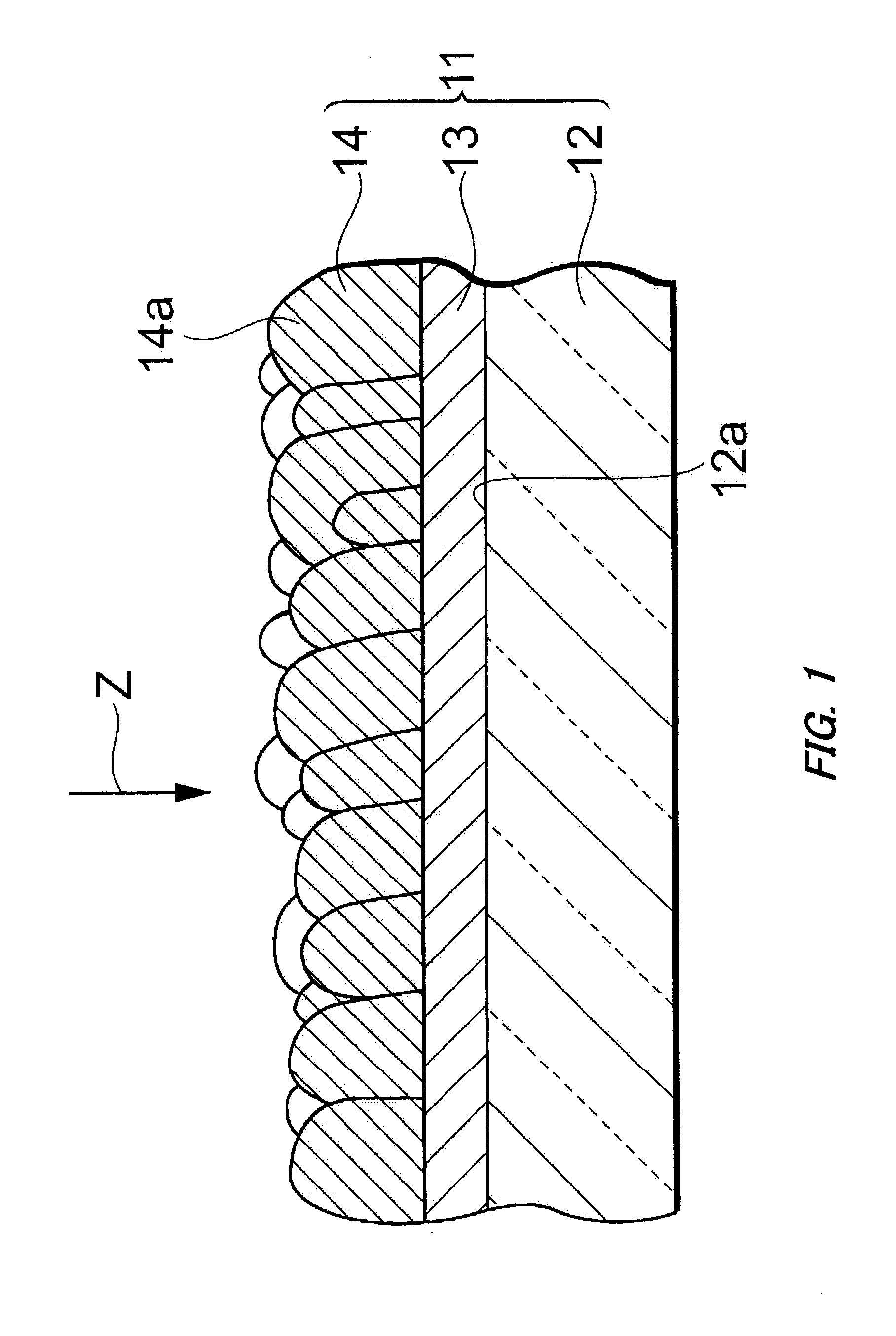
[0035]FIG. 1 is a schematic sectional view schematically showing an embodiment of an electrode for photoelectric conversion elements according to the present invention. An electrode for photoelectric conversion elements 11 in this embodiment has a structure in which a porous metal oxide layer 14 containing zinc oxide formed by electrolytic deposition is provided on a base 12 having a conductive surface 12a. The metal oxide layer 14 has a plurality of bump-like protrusions 14a formed so as to protrude radially from the base side, and also has an emission peak in the region of 350 to 400 nm in cathodoluminescence measurement. Though a dye-sensitized solar cell is described as an example of a photoelectric conversion element in this embodiment, the photoelectric conversion element is not limited to such.
[0036]A size and shape of the base 12 are not particularly limited so long as the base 12 is capable of supporting at least the metal oxide layer 14. For instance, a plate-like base or ...
second embodiment
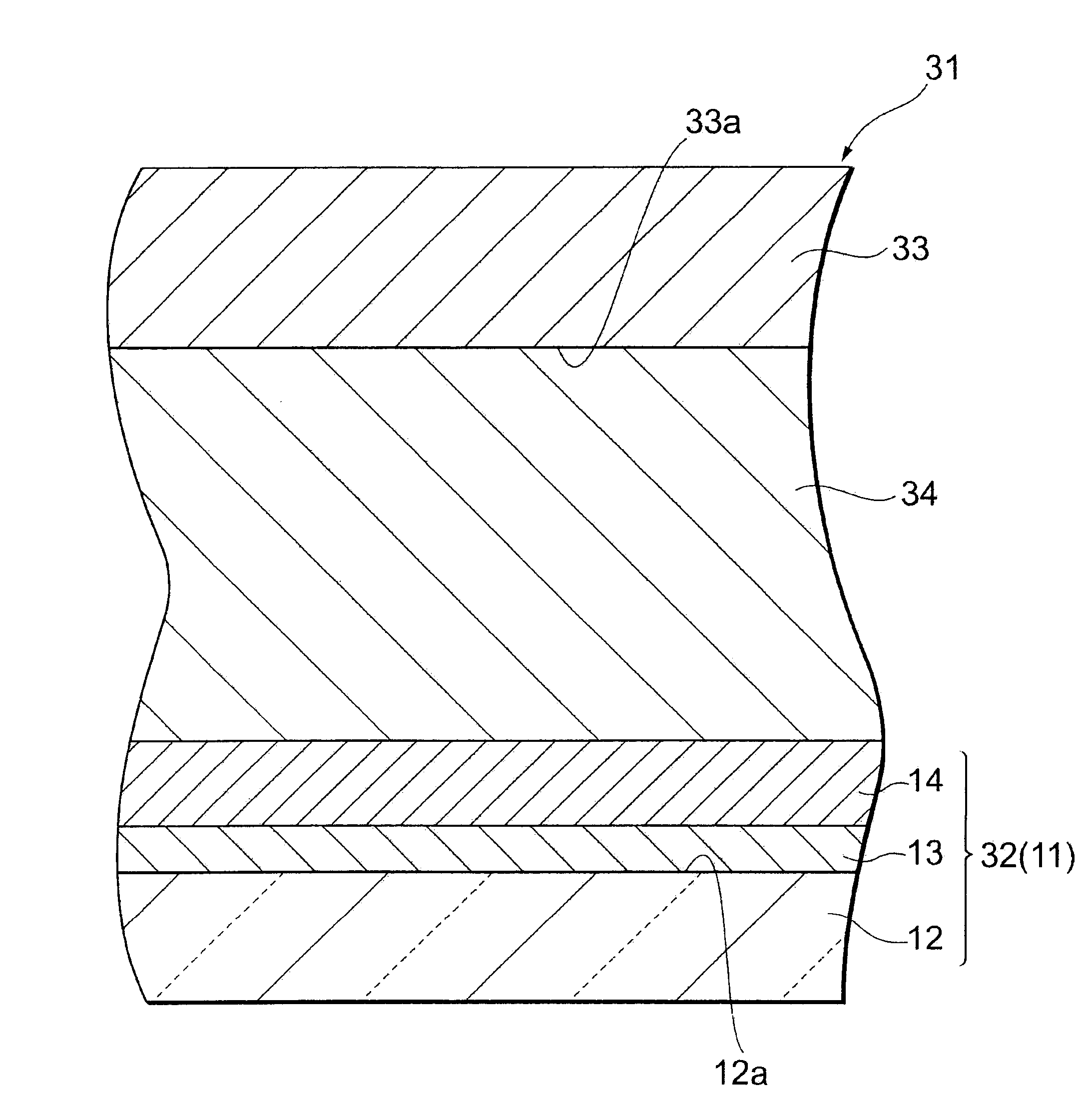
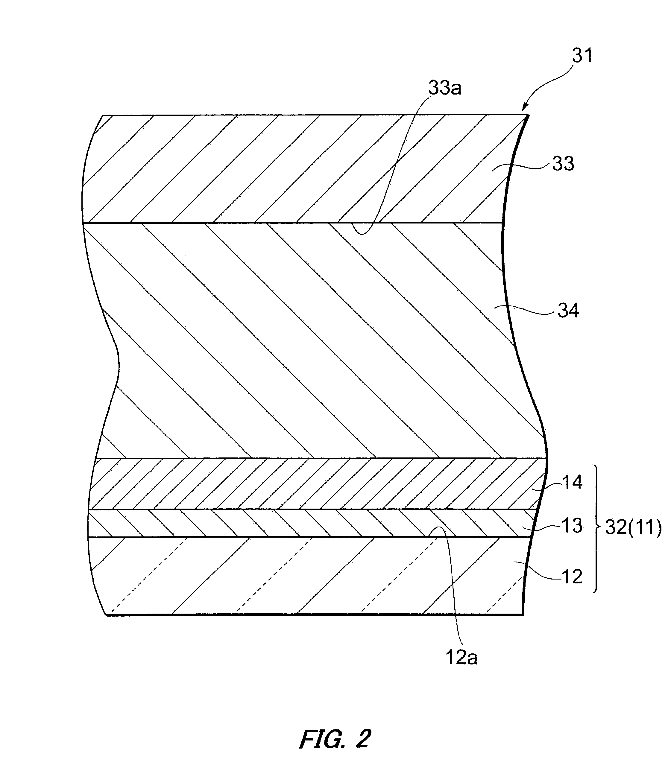
[0067]FIG. 2 is a schematic sectional view schematically showing an embodiment of a dye-sensitized solar cell according to the present invention. A dye-sensitized solar cell 31 (solar cell) includes, as a photoelectric conversion electrode (element), a working electrode 32 in which the second dye is re-adsorbed (carried) on the metal oxide layer 14 of the electrode for photoelectric conversion elements 11 described in the first embodiment. The dye-sensitized solar cell 31 includes this working electrode 32, a counter electrode 33 disposed so as to face the working electrode 32, and a charge transport layer 34 disposed between the working electrode 32 and the counter electrode 33.
[0068]The counter electrode 33 has its conductive surface 33a facing the metal oxide layer 14 to which the second dye is adsorbed. A known electrode may be appropriately adopted as the counter electrode 33. For example, a structure in which a conductive film is provided on a transparent substrate, a structur...
examples
[0071]The following describes the present invention in detail by way of Examples, though the present invention is not limited to such.
PUM
| Property | Measurement | Unit |
|---|---|---|
| voltage | aaaaa | aaaaa |
| haze | aaaaa | aaaaa |
| temperature | aaaaa | aaaaa |
Abstract
Description
Claims
Application Information