Fabrication and structure of asymmetric field-effect transistors using L-shaped spacers

a field-effect transistor and spacer technology, applied in the field of semiconductor technology, can solve the problems of weakened analog performance, difficult to integrate choi's process into a larger semiconductor process, and the inability to control the operation of the igfet with its gate electrode, etc., and achieve the effects of low cost, low cost, and high transconductan

Active Publication Date: 2010-09-30
NAT SEMICON CORP
View PDF25 Cites 157 Cited by
  • Summary
  • Abstract
  • Description
  • Claims
  • Application Information

AI Technical Summary

Benefits of technology

[0053]The first and second main S/D portions normally respectively function as a main source portion and a main drain portion. In that case, the pocket portion is a source-side pocket portion. When the IGFET has two lateral extensions respectively functioning as source and drain extensions, the drain extension is preferably more lightly doped than the source extension. This reduces damaging drain-side hot-carrier injection into the gate dielectric layer while enabling the IGFET to have a high transconductance in the presence of the source resistance.

Problems solved by technology

When surface or bulk punchthrough occurs, the operation of the IGFET cannot be controlled with its gate electrode.
However, Choi's coupling of the formation of gate electrode 46 with the formation of source/drain extensions 26E and 28E in the process of FIG. 8 is laborious and could make it difficult to incorporate Choi's process into a larger semiconductor process that provides other types of IGFETs.
Although it would be economic

Method used


Image

  • Fabrication and structure of asymmetric field-effect transistors using L-shaped spacers
  • Fabrication and structure of asymmetric field-effect transistors using L-shaped spacers
  • Fabrication and structure of asymmetric field-effect transistors using L-shaped spacers

Examples


Embodiment Construction

List of Contents

[0070]A. Reference Notation and Other Preliminary Information

[0071]B. Complementary-IGFET Structures Suitable for Mixed-signal Applications

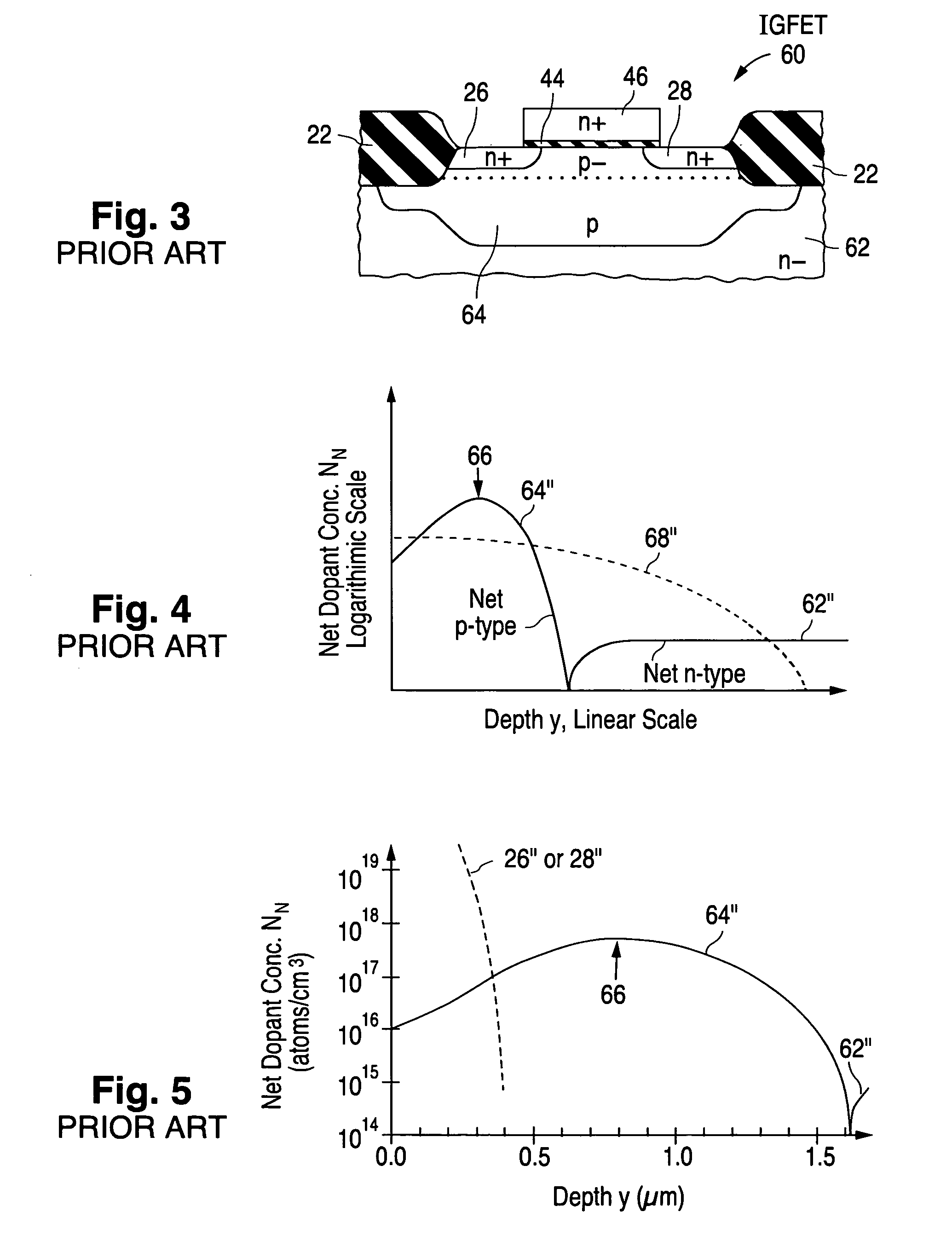
[0072]C. Well Architecture and Doping Characteristics

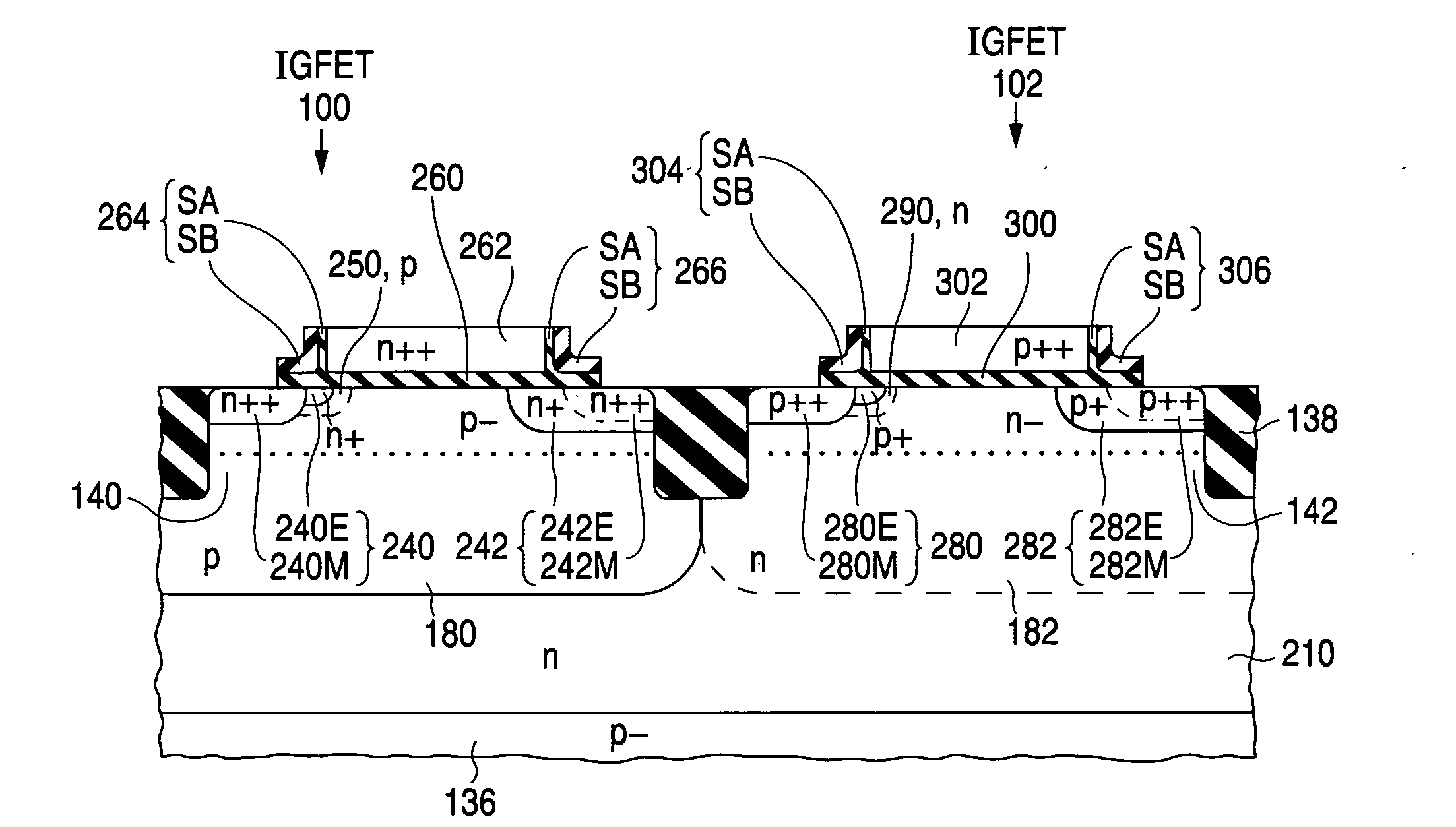
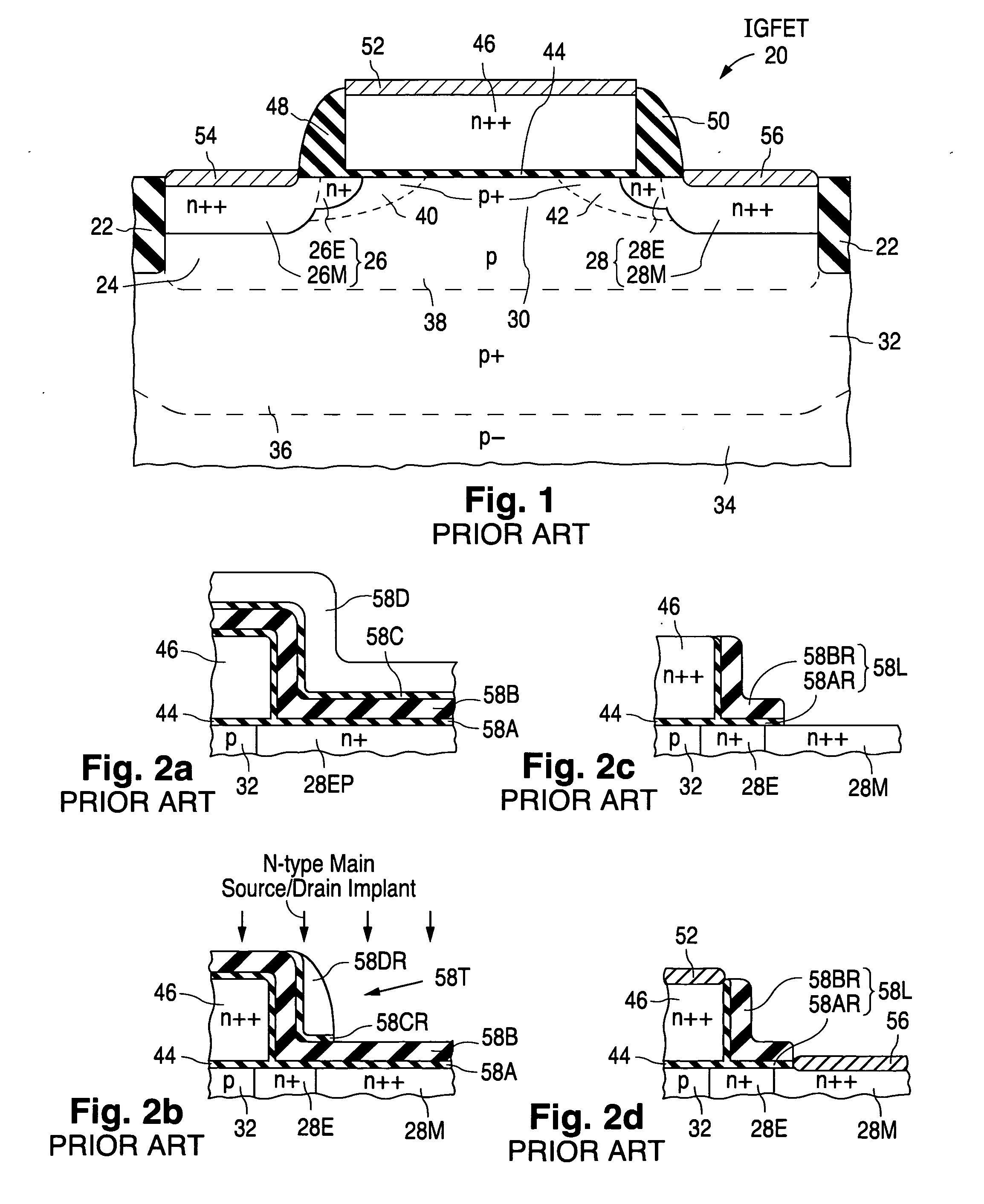
[0073]D. Asymmetric High-voltage IGFETs[0074]D1. Structure of Asymmetric High-voltage N-channel IGFET[0075]D2. Source / Drain Extensions of Asymmetric High-voltage N-channel IGFET[0076]D3. Structure of Asymmetric High-voltage P-channel IGFET[0077]D4. Source / Drain Extensions of Asymmetric High-voltage P-channel IGFET

[0078]E. Extended-drain IGFETs[0079]E1. Structure of Extended-drain N-channel IGFET[0080]E2. Operational Physics of Extended-drain N-channel IGFET[0081]E3. Structure of Extended-drain P-channel IGFET[0082]E4. Operational Physics of Extended-drain P-channel IGFET

[0083]F. Information Generally Applicable to All of Present IGFETs

[0084]G. Fabrication of Complementary-IGFET Structure Suitable for Mixed-signal Applications[0085]G1. General Fabrication Information[0086]G2. Wel...


PUM


Abstract

Fabrication of an asymmetric field-effect transistor (100) entails defining a gate electrode (262) above, and vertically separated by a gate dielectric layer (260) from, a channel-zone portion (244) of body material of a semiconductor body. Semiconductor dopant is introduced into the body material to define a more heavily doped pocket portion (250) using the gate electrode as a dopant-blocking shield. A spacer (264T) is provided along the gate electrode. The spacer includes (i) a dielectric portion situated along the gate electrode, (ii) a dielectric portion situated along the semiconductor body, and (iii) a filler portion (SC) largely occupying the space between the other two spacer portions. Semiconductor dopant is introduced into the semiconductor body to define a pair of main source/drain portions (240M and 240E) using the gate electrode and the spacer as a dopant-blocking shield. The filler spacer portion is removed to convert the spacer to an L shape (264). A pair of electrical contacts are formed respectively to the main S/D portions.

Description

CROSS-REFERENCE TO RELATED APPLICATIONS[0001]This application is related to the following U.S. patent applications all filed on the same date as this application: U.S. patent application Ser. No. ______ (Bulucea et al.), attorney docket no. NS-7005 US, U.S. patent application Ser. No. ______ (Bulucea et al.), attorney docket no. NS-7040 US, U.S. patent application Ser. No. ______ (Bahl et al.), attorney docket no. NS-7210 US, U.S. patent application Ser. No. ______ (Yang et al.), attorney docket no. NS-7307 US, U.S. patent application Ser. No. ______ (Yang et al.), attorney docket no. NS-7313 US, and U.S. patent application Ser. No. ______ (Bulucea et al.), attorney docket no. NS-7433 US, U.S. patent application Ser. No. ______ (Bulucea et al.), attorney docket no. NS-7434 US, U.S. patent application Ser. No. ______ (French et al.), attorney docket no. NS-7435 US, U.S. patent application Ser. No. ______ (Bulucea et al.), attorney docket no. NS-7436 US, and U.S. patent application Se...

Claims


Application Information

Patent Timeline
IPC IPC(8): H01L29/78H01L21/336
CPCH01L21/26513H01L29/6656H01L21/26586H01L21/823807H01L21/823814H01L21/823892H01L27/0922H01L29/0653H01L29/0847H01L29/1045H01L29/105H01L29/1083H01L29/518H01L29/66659H01L29/7835H01L29/665H01L29/6653H01L21/2652H01L21/2658H01L21/823864
Inventor PARKER, D. COURTNEYARCHER, DONALD M.BAHL, SANDEEP R.BULUCEA, CONSTANTINFRENCH, WILLIAM D.JOHNSON, PETER B.YANG, JENG-JIUN
Owner NAT SEMICON CORP
Why Eureka
Try Eureka