Epitaxial growth method

a growth method and single-wallet technology, applied in the direction of crystal growth process, polycrystalline material growth, chemically reactive gas, etc., can solve the problems of insufficient growth apparatus, poor film thickness shape, and inability to obtain excellent film thickness distribution, etc., to improve the quality of the back surface improve the quality of the epitaxial wafer, and reduce the frequency of cleaning the inside of the reaction chamber

Active Publication Date: 2010-10-07
SHIN-ETSU HANDOTAI CO LTD
View PDF1 Cites 5 Cited by
  • Summary
  • Abstract
  • Description
  • Claims
  • Application Information

AI Technical Summary

Benefits of technology

[0017]The present invention has been made in view of the problems described above, and an object thereof is to provide a single wafer processing epitaxial growth method that can obtain the effects, such as an increase in the quality of an epitaxial wafer and an increase in productivity, which are produced by the degree of the flow rate of carrier gas, and deposit an epitaxial layer on a single crystal substrate without deforming the film thickness shape.

Problems solved by technology

However, when epitaxial growth is performed by using such an epitaxial growth apparatus 101, the film thickness of an epitaxial layer deposited on a single crystal becomes nonuniform, leading to a problem with a film thickness shape.
However, even when such an epitaxial growth apparatus 101′ is used, an excellent film thickness shape (film thickness distribution) may not be obtained, and this growth apparatus is inadequate.
In addition, there is a considerable individual difference among the upper walls of the reaction chambers, and the upper walls have various shapes microscopically.
This makes the film thickness of the epitaxial layer near the outer edge of the single crystal substrate particularly small (results in the generation of the peripheral sag), lowering the degree of flatness.
However, in this case, it is known that the film thickness shape has a thick peripheral part, also lowering the degree of flatness.

Method used


Image

  • Epitaxial growth method
  • Epitaxial growth method
  • Epitaxial growth method

Examples


Embodiment Construction

[0042]Hereinafter, an embodiment of the present invention will be described; however, the present invention is not limited thereto.

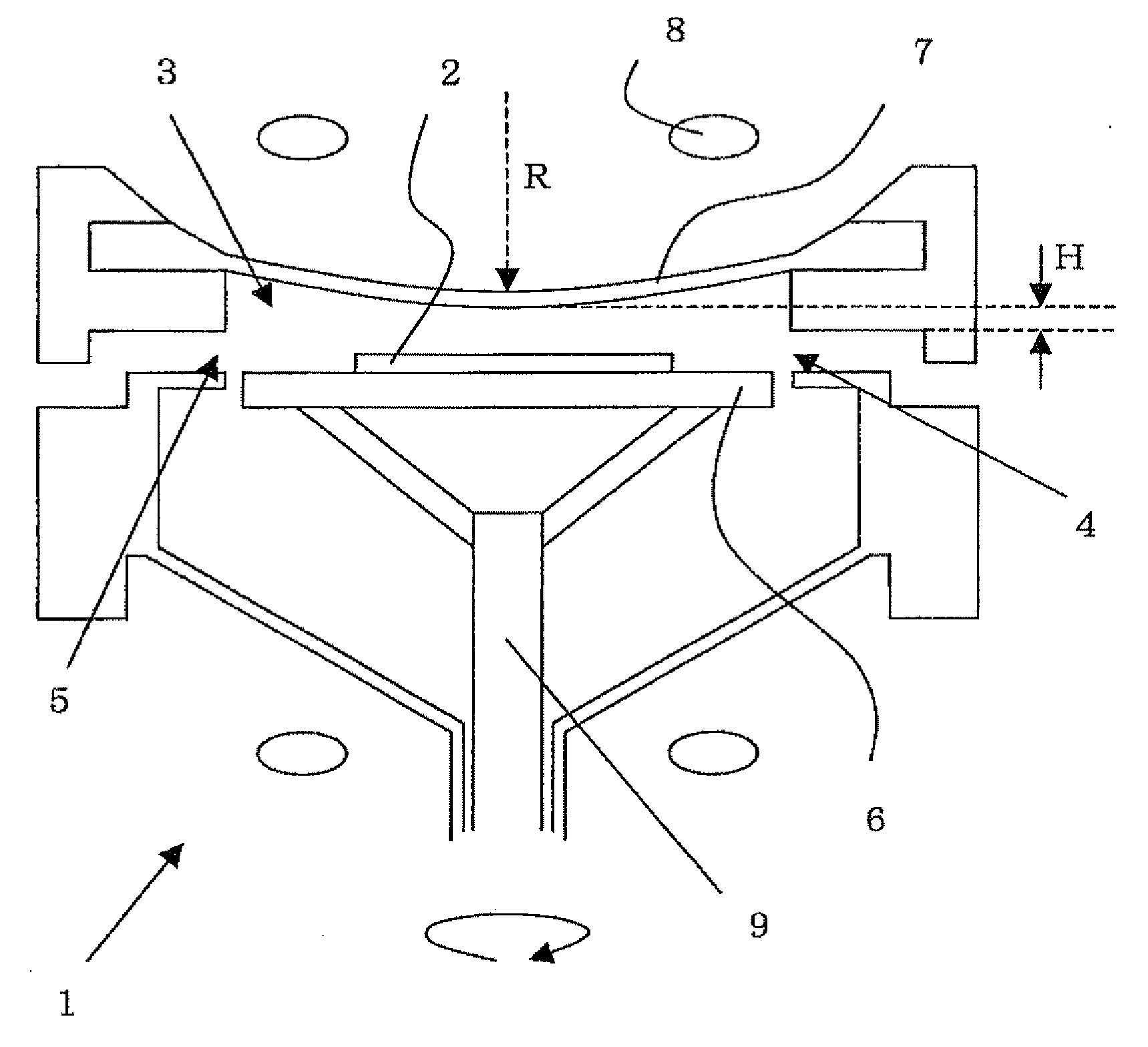
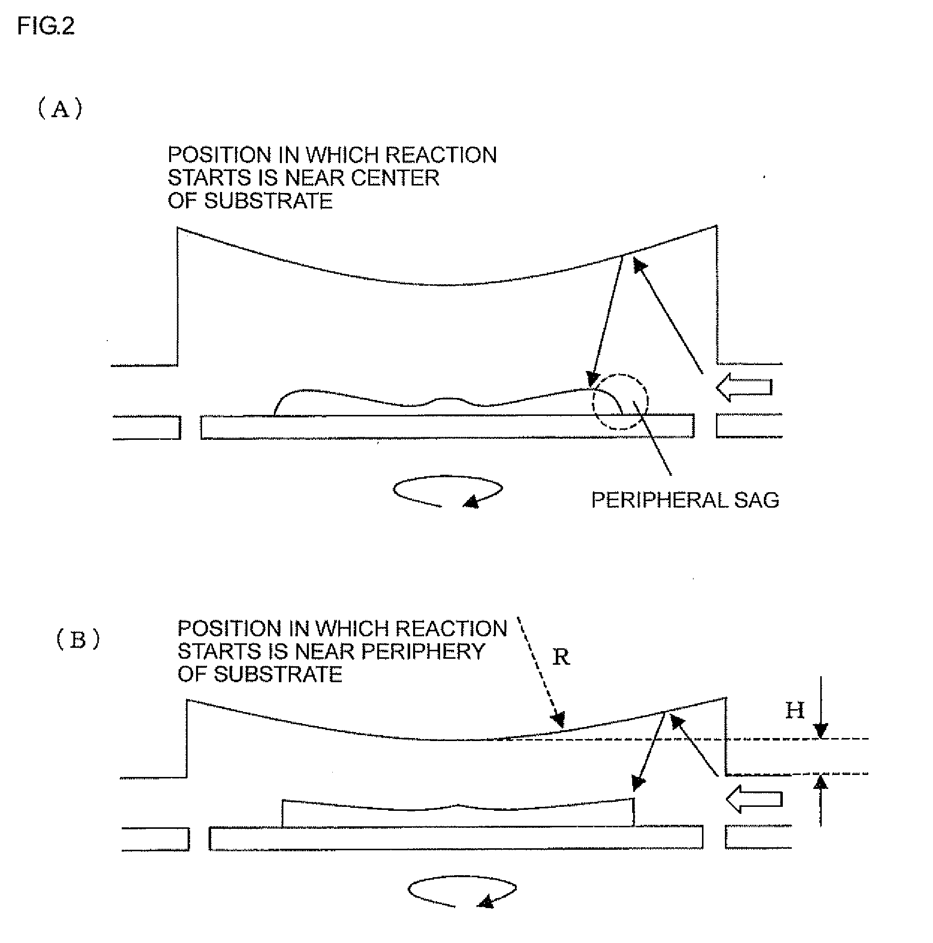
[0043]First, the inventor conducted a study of the film thickness distribution of an epitaxial layer deposited on a single crystal substrate by a conventional epitaxial growth method by using a single wafer processing epitaxial growth apparatus in which an upper wall of a reaction chamber had a downward convexity as shown in FIG. 9. Incidentally, here, trichlorosilane was used as raw material gas, hydrogen was used as carrier gas, and a silicon single crystal layer was deposited on a silicon single crystal substrate.

[0044]The results of the study revealed that the vertical section of the silicon single crystal layer had a shape shown in FIG. 2(A), and the film thickness distribution was nonuniform. That is, as was obvious from the shape of the vertical section, the silicon single crystal layer had a relatively thick layer in the center and outer region o...


PUM

PropertyMeasurementUnit
diameteraaaaaaaaaa
heightaaaaaaaaaa
heightaaaaaaaaaa

Abstract

The invention provides an epitaxial growth method which is a single wafer processing epitaxial growth method by which at least a single crystal substrate is placed in a reaction chamber with an upper wall having a downward convexity and an epitaxial layer is deposited on the single crystal substrate by introducing raw material gas and carrier gas into the reaction chamber through a gas feed port, in which, after any one of the radius of curvature of the upper wall of the reaction chamber and a difference between an upper end of the gas feed port and a lower end of the upper wall of the reaction chamber in the height direction or both are adjusted in accordance with the flow rate of the carrier gas which is introduced into the reaction chamber through the gas feed port, an epitaxial layer is deposited on the single crystal substrate. As a result, a single wafer processing epitaxial growth method is provided that can obtain the effects, such as an increase in the quality of an epitaxial wafer and an increase in productivity, which are produced by the degree of the flow rate of carrier gas, and deposit an epitaxial layer on a single crystal substrate without deforming the film thickness shape.

Description

TECHNICAL FIELD[0001]The present invention relates to a single wafer processing epitaxial growth method by which an epitaxial layer is deposited on a single crystal substrate.BACKGROUND ART[0002]An epitaxial growth technique is a technique of obtaining a single crystal thin film layer by vapor deposition, the single crystal thin film layer used in production of an integrated circuit such as a MOSLSI or a bipolar transistor, and is a highly important technique because the technique makes it possible to grow a uniform single crystal thin film on a clean semiconductor single crystal substrate according to a crystal orientation of the substrate and form a steep impurity gradient at a junction where there is a great difference in dopant concentration.[0003]As a typical apparatus for performing such epitaxial growth, there are three types of apparatuses: a vertical (pancake) type, a barrel (cylinder) type, and a horizontal type. These growth apparatuses have common basic principles. The g...

Claims


Application Information

Patent Timeline
Patent Type & Authority Applications(United States)
IPC IPC(8): C30B23/02
CPCC23C16/44C30B25/14C30B25/08
Inventor OHNISHI, MASATO
Owner SHIN-ETSU HANDOTAI CO LTD
Why Eureka
Try Eureka