

Drive circuit of semiconductor device
a technology of drive circuit and semiconductor device, which is applied in the direction of pulse technique, power conversion system, oscillation generator, etc., can solve the problems of large surge voltage generation, and achieve the effect of reducing the loss and noise of the inverter, and reducing the switching loss of the power semiconductor devi
- Summary
- Abstract
- Description
- Claims
- Application Information
AI Technical Summary
Benefits of technology
Problems solved by technology
Method used
Image

Examples
embodiment 1
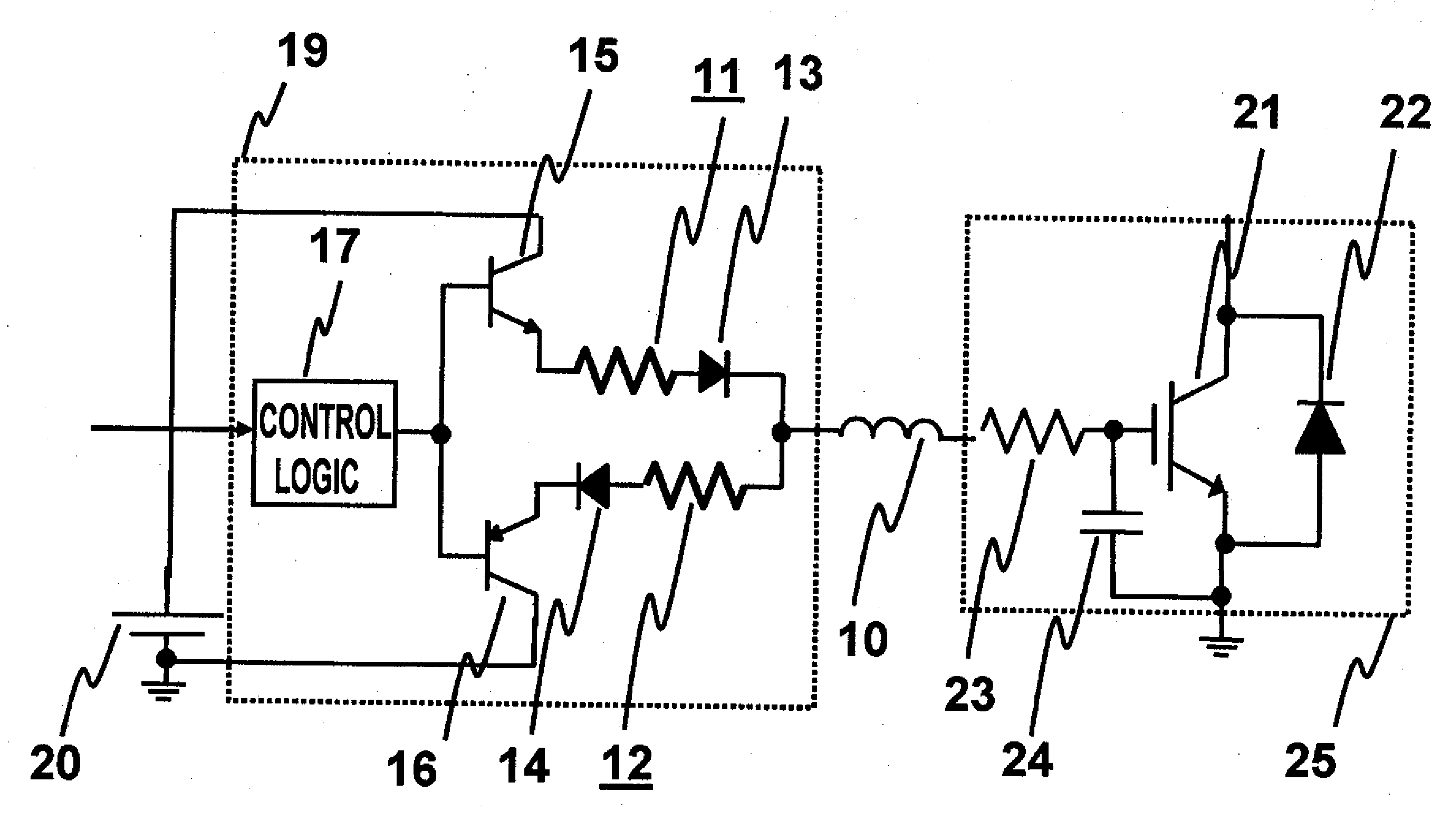
[0028]FIG. 1 is a block diagram of a drive circuit of a power semiconductor device according to a, first preferred embodiment of the present invention. A main circuit of an inverter is composed of Si-IGBT 21 and SiC-SBD 22. Si-IGBT has a buried resistance (Rgin) 23 and an IGBT input capacitance (Cies) 24 built into the IGBT. The Si-IGBT 21 and 22 of the main circuit are driven via a drive circuit 19 according to the present invention and a drive circuit power supply 20. According to the present drive circuit, an on-side gate resistance 11 is set to be smaller than an off-side gate resistance 12.
[0029]The SiC-SBD 22 has a breakdown voltage strength as high as approximately 10 times that of Si, and therefore, a drift layer for ensuring pressure resistance can be reduced to approximately 1 / 10, so that the on-voltage of the power device can be reduced. Thus, SiC and other wide bandgap semiconductor devices can use unipolar devices even in high pressure resistance areas where Si semicond...
embodiment 2
[0036]FIG. 7 shows a block diagram of a drive circuit of a power semiconductor device according to a second preferred embodiment of the present invention. The same reference numbers are used to denote the same components as embodiment 1. According to the drive circuit of the present invention, in addition to setting the on-side gate resistance 11 smaller than the off-side gate resistance 12, a speed-up capacitor 18 is further provided.
[0037]FIG. 8 shows a gate voltage waveform of a drive circuit according to the second embodiment of the present invention. The gate input capacitance is set to 110 nC, the gate buried resistance is set to 1.0Ω, and the on-side gate resistance is set to 1.0Ω. The turn-on time from the gate voltage rise time is 0.5 μs when the speed-up capacitor 18 is not provided, whereas the turn-on time from the gate voltage rise time can be reduced to approximately half or 0.3 μs by providing the speed-up capacitor 12 μF, according to which high speed drive of IGBT b...
embodiment 3
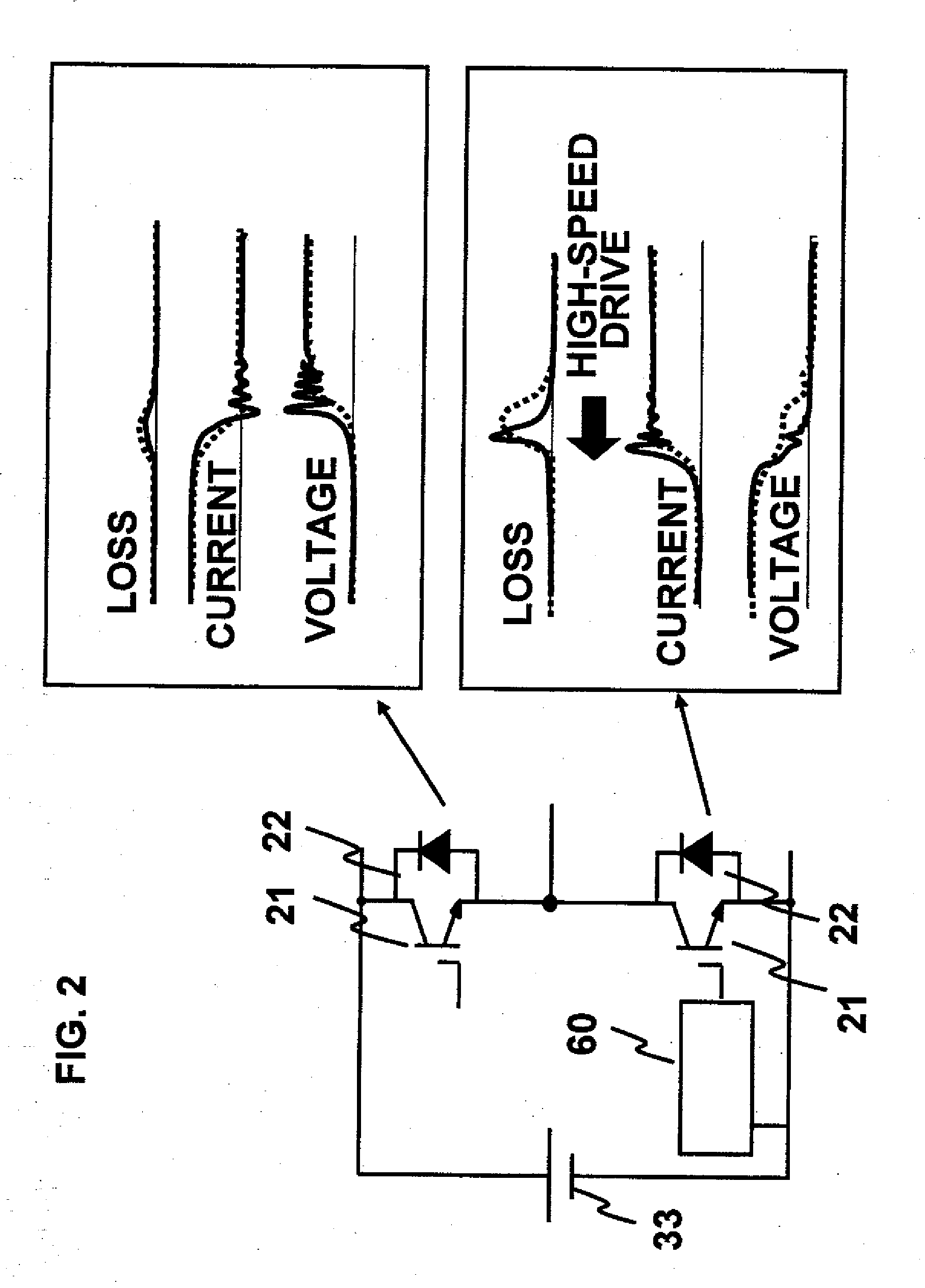
[0038]FIG. 9 shows a block diagram of an inverter circuit according to a third preferred embodiment of the present invention. The same components as embodiment 1 are denoted by the same reference numbers. According to the present inverter, power modules 25 are connected in series to constitute a portion corresponding to a single phase of the inverter. The inverter further comprises a main circuit power supply 33 of the inverter, and parasitic inductances 34 and 35 disposed between the power modules 25 and the main circuit power supply 33. According to the power module 25 of the present invention, a high-voltage side terminal 51 of the IGBT and the high-voltage side terminal 52 of the SiC-SBD are provided individually, and an inductance 31 is provided between the high-voltage side terminal 51 of the IGBT and the high-voltage side terminal 52 of the SiC-SBD.
[0039]FIG. 10 shows an equivalent circuit diagram of a main circuit of the inverter. A sum of the parasitic inductance 34 and 35 ...
PUM
 Abstract
Description
Claims
Application Information