Nitride semi-conductor light emitting device

a semi-conductor and light-emitting technology, which is applied in the manufacture of semiconductor/solid-state devices, semiconductor devices, electrical apparatus, etc., can solve the problems of small external quantum efficiency and light output, low light emission efficiency in light emission layer, and low internal quantum efficiency of nitride semi-conductor (nitride mixed crystal) , to achieve the effect of improving the quality of algainn crystal and high internal quantum efficiency

Active Publication Date: 2010-10-28
MATSUSHITA ELECTRIC WORKS LTD +1
View PDF4 Cites 23 Cited by
  • Summary
  • Abstract
  • Description
  • Claims
  • Application Information

AI Technical Summary

Benefits of technology

[0015]The nitride semi-conductor light emitting device is preferably produced by steps of forming the p-type nitride semi-conductor layer, the n-type nitride semi-conductor layer, and the light emission layer between the p-type nitride semi-conductor layer and the n-type nitride semi-conductor layer, respectively within the chamber by metal organic vapor phase epitaxy (MOVPE). The forming steps are performed so as to develop within the light emission layer the AlGaInN quantum well structure including the well layer and the barrier layer, in which the barrier layer has a higher concentration of Al than the well layer. The process is characterized by supplying an impurity (preferably Si) and Al simultaneously into the chamber when growing at least the barrier layer in order to entrap oxygen with the impurity. The process enables to reduce the amount of oxygen combined with Al in the chamber of MOPVE apparatus, thereby improving quality of AlGaInN crystal as the light emission layer, so as to effectively supply the well layer with electrons for achieving a high internal quantum efficiency in the light emission layer.

Problems solved by technology

The very small external quantum efficiency and light output have been obstacles to practical use of the light emitting device in UV region, and are possibly attributed to very low light emission efficiency in light emission layer (referred to as internal quantum efficiency, hereafter).
Due to transition, point defect, and unintended impurity which are formed in large amount in the light emission layer, the nitride semi-conductor (nitride mixed crystal) has very low internal quantum efficiency.
Especially, ternary mixed crystal including Al such as AlGaN has considerably low internal quantum efficiency, for difficulty in growth of the mixed crystal with high quality.
Besides, Al needs to be added in large amount in growth of AlGaInN layer for achieving light emission in short wavelength, but Al easily entraps the unwanted oxygen.
The entrapped oxygen tends to generate defects, to degenerate layers, and to form undesirable energy levels, thereby decreasing the internal quantum yield of light emission layer.

Method used


Image

  • Nitride semi-conductor light emitting device
  • Nitride semi-conductor light emitting device
  • Nitride semi-conductor light emitting device

Examples


Embodiment Construction

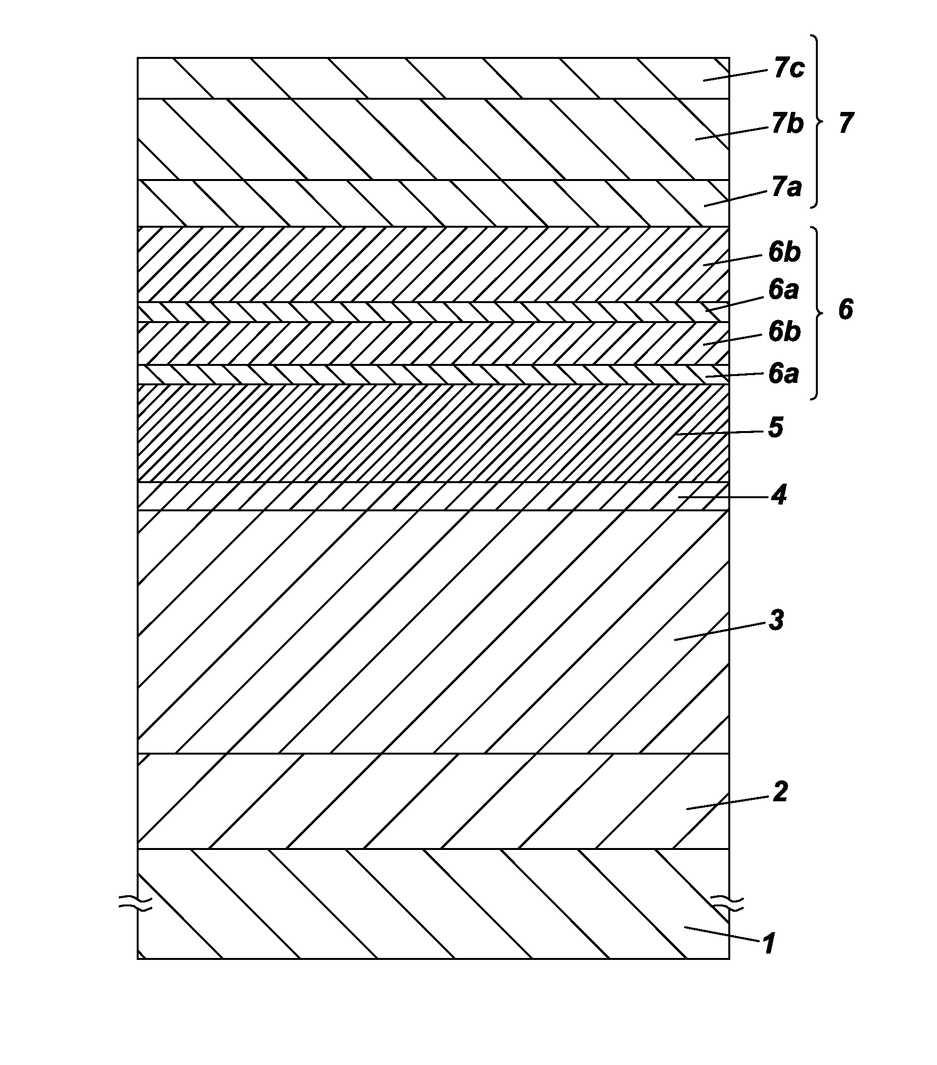
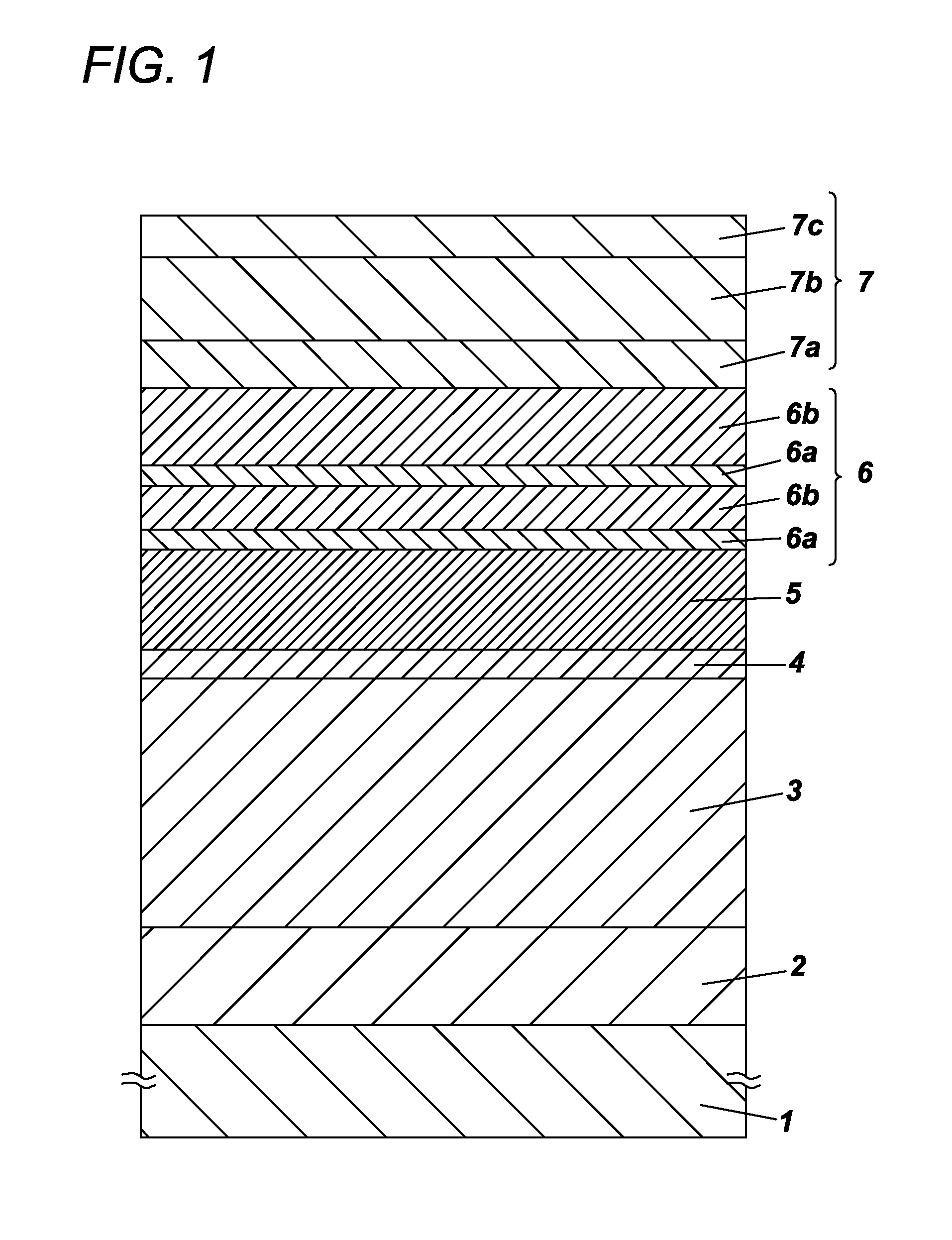
[0020]A nitride semi-conductor light emitting device in this embodiment is a UV-LED and includes a single crystal substrate 1 for epitaxial growth, a first buffer layer 2, an n-type nitride semiconductor layer 3, a second buffer layer 4, a third buffer layer 5, a light emission layer 6, and a p-type nitride semi-conductor layer 7, which are superimposed in this order on the single crystal substrate 1, as shown in FIG. 1. A cathode (not shown) and an anode (not shown) are provided respectively on the n-type nitride semiconductor layer 3 and the p-type nitride semiconductor layer 7.

[0021]The single crystal substrate 1 is formed of a sapphire substrate with a (0001) surface (i.e., c-surface) serving as a mounting surface.

[0022]The first buffer layer 2 is formed of a single crystal of AlN layer having its thickness of 2.5 μm, acting to suppress threading dislocation and residual distortion of the n-type nitride semi-conductor layer 3. The thickness of first buffer 2 is not limited to 2....


PUM


Abstract

A nitride semi-conductor light emitting device has a p-type nitride semi-conductor layer 7, an n-type nitride semi-conductor layer 3, and a light emission layer 6 which is interposed between the p-type nitride semi-conductor layer 7 and the n-type nitride semi-conductor layer 3. The light emission layer 6 has a quantum well structure with a barrier layer 6b and a well layer 6a. The barrier layer 6b is formed of AlaGabIn(1-a-b)N (0<a<1, 0<b<1, 1−a−b>0), and contains a first impurity at a concentration of A greater than zero. The well layer 6a is formed of AlcGadIn(1-c-d)N (0<c<1, c<a, 0<d<1, 1−c−d>0), and contains a second impurity at a concentration of B equal to or greater than zero. In the nitride semi-conductor light emitting device of the present invention, the concentration of A is larger than that of B, in order that the barrier layer 6b has a concentration of oxygen smaller than that in the well layer 6a.

Description

TECHNICAL FIELD[0001]This invention relates to a nitride semi-conductor light emitting device including an AlGaInN layer.BACKGROUND ART[0002]A nitride semi-conductor light emitting device which emits light in UV-visible region is expected to be widely applied, hygienically, medically, industrially, and has been studied to develop an illumination device, a precision machine or the like, for its compact size and its low electrical consumption. The light emitting device which emits light in specific region including blue-color region has already been developed for practical use.[0003]For development of the nitride semi-conductor light emitting device (including that emitting blue light which is referred to as a blue-color light emitting diode), it is necessary to further improve its light emission efficiency and light output. At present, the semi-conductor light emitting device provides much smaller external quantum efficiency and light output in UV region than blue-color region. The v...

Claims


Application Information

Patent Timeline
Patent Type & Authority Applications(United States)
IPC IPC(8): H01L33/00
CPCH01L33/32H01L33/06
Inventor TAKANO, TAKAYOSHITSUBAKI, KENJIHIRAYAMA, HIDEKIFUJIKAWA, SACHIE
Owner MATSUSHITA ELECTRIC WORKS LTD
Why Eureka
Try Eureka