Method of enhancing the conductive and optical properties of deposited indium tin oxide (ITO) thin films

a technology thin film, which is applied in the field of improving the conductive and optical properties of indium tin oxide (ito or insnox) thin film, can solve the problems of loss of conductivity, loss of conductive sputter-deposited tcos such as znalo/sub>x and ito formed in a conventional sputtering process, and inability to pyrolysis deposited tcos,

Inactive Publication Date: 2010-12-02
GUARDIAN GLASS LLC
View PDF10 Cites 31 Cited by
  • Summary
  • Abstract
  • Description
  • Claims
  • Application Information

AI Technical Summary

Benefits of technology

[0006]Thus, it will be appreciated that there is a need in the art for techniques for making or forming a TCO electrode in a manner that improves the TCO's electrical conductivity as deposited and/or after high temperature processing.
[0007]It is known that lower sheet resistance in ITO films in comparison to its as-deposited counterpart typically requires activation. The activation, in turn, typically is achieved by baking in air in the temperature range of 300-350 degrees C. for 30-120 minutes. The inventors of the instant invention, however, have discovered that baking ITO films in a low oxygen environment such as a vacuum can further reduce the resistivity in comparison to air baked samples. Surprisingly and unexpectedly, the reduction in resistivity has been as

Problems solved by technology

However, from the viewpoint of uniformity, potential cost savings, and film smoothness, pyrolytically deposited TCOs are not desirable.
Unfortunately, conductive sputter-deposited TCOs such as ZnAlOx and ITO formed in a conventional sputtering process tends to lose significant am

Method used


Image

  • Method of enhancing the conductive and optical properties of deposited indium tin oxide (ITO) thin films
  • Method of enhancing the conductive and optical properties of deposited indium tin oxide (ITO) thin films
  • Method of enhancing the conductive and optical properties of deposited indium tin oxide (ITO) thin films

Examples


Embodiment Construction

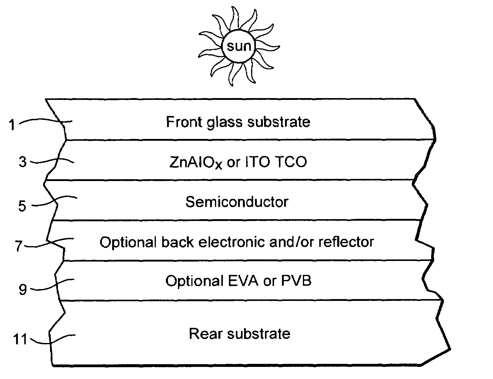
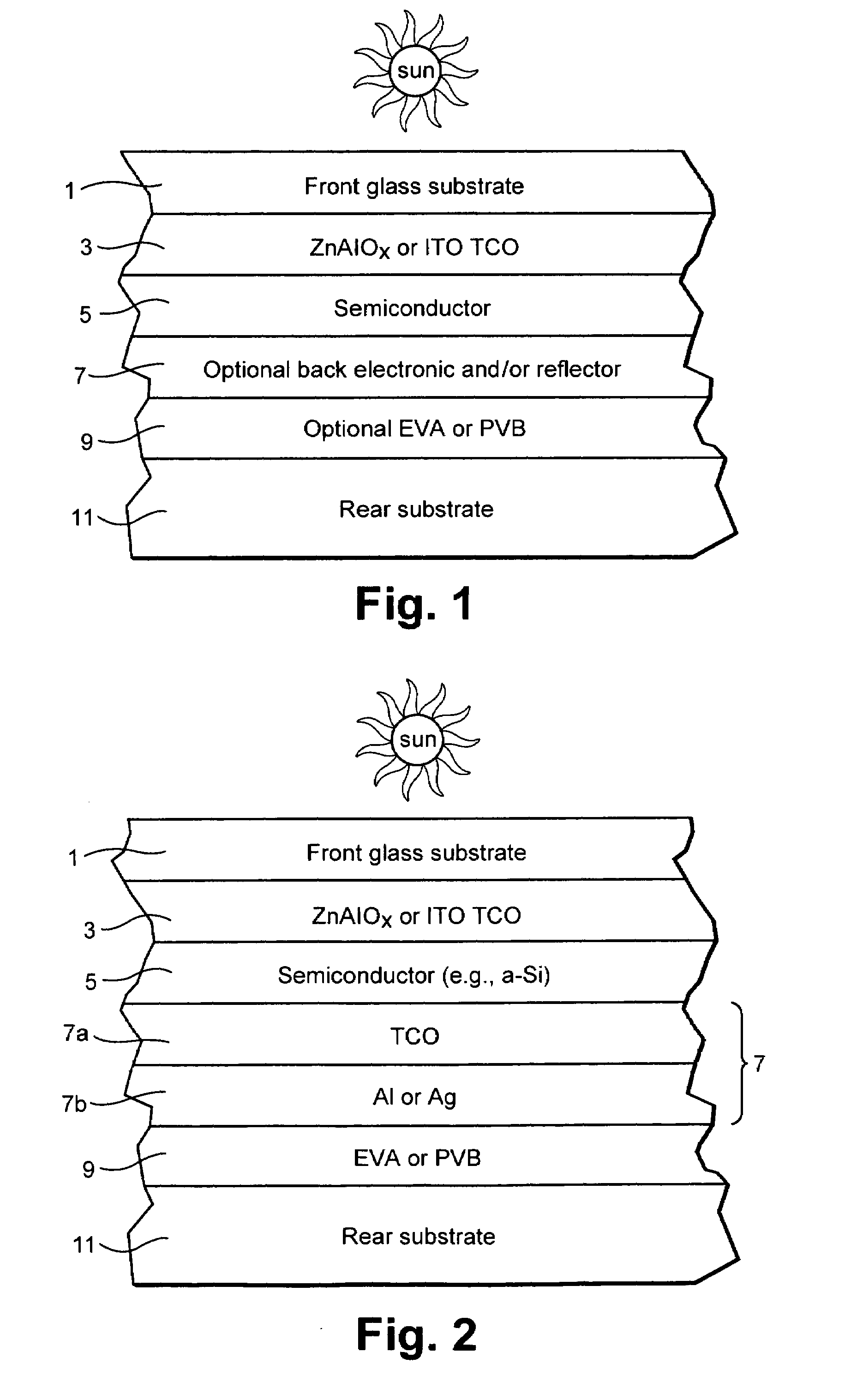
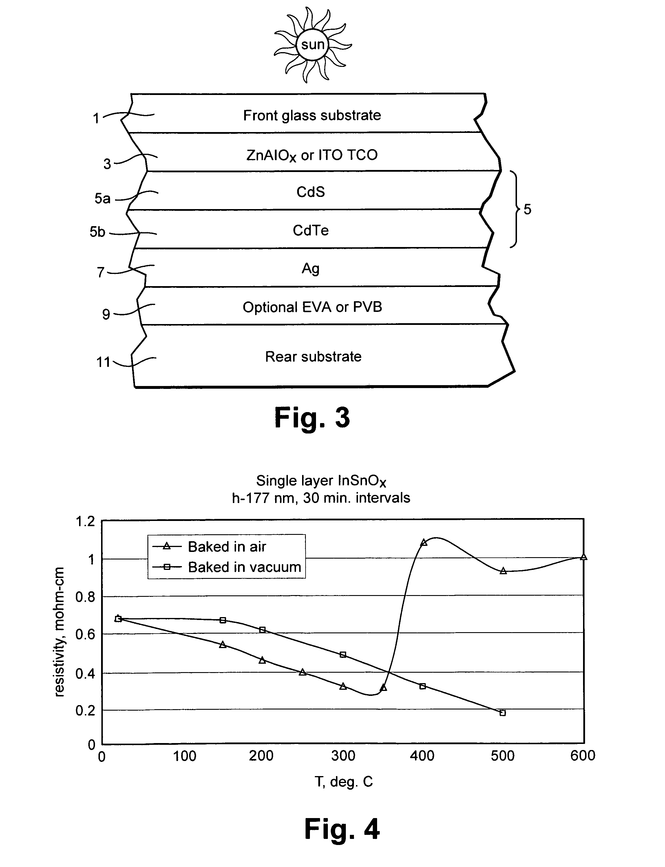
[0019]Photovoltaic devices such as solar cells convert solar radiation and other light into usable electrical energy. The energy conversion occurs typically as the result of the photovoltaic effect. Solar radiation (e.g., sunlight) impinging on a photovoltaic device and absorbed by an active region of semiconductor material (e.g., a semiconductor film including one or more semiconductor layers such as a-Si layers, or any other suitable semiconductor material) generates electron-hole pairs in the active region. The electrons and holes may be separated by an electric field of a junction in the photovoltaic device. The separation of the electrons and holes by the junction results in the generation of an electric current and voltage. In certain example embodiments, the electrons flow toward the region of the semiconductor material having n-type conductivity, and holes flow toward the region of the semiconductor having p-type conductivity. Current can flow through an external circuit con...


PUM

PropertyMeasurementUnit
Fractionaaaaaaaaaa
Wavelengthaaaaaaaaaa
Optical reflectivityaaaaaaaaaa

Abstract

Certain example embodiments of this invention relate to a method of activating an indium tin oxide (ITO) thin film deposited, directly or indirectly, on a substrate. The ITO thin film is baked in a low oxygen environment at a temperature of at least 450 degrees C. for at least 10 minutes so as to provide for (1) a post-baked resistivity of the ITO thin film that is below a resistivity of a corresponding air-baked ITO thin film, (2) a post-baked visible spectrum absorption and transmission of the ITO thin film that respectively are below and above the absorption and transmission of the corresponding air-baked ITO thin film, and (3) a post-baked infrared reflectivity of the ITO thin film that is above the reflectivity of the corresponding air-baked ITO thin film. The substrate with the activated ITO thin film may be used in a photovoltaic device, for example.

Description

FIELD OF THE INVENTION[0001]Certain example embodiments of this invention relate to processes for improving the conductive and optical properties of indium tin oxide (ITO or InSnOx) thin films. More particularly, certain example embodiments of this invention relate to processes for reducing the sheet resistance of ITO thin films by baking a sample in a low oxygen or vacuum environment at an elevated temperature.BACKGROUND AND SUMMARY OF EXAMPLE EMBODIMENTS OF THE INVENTION[0002]Photovoltaic devices are known in the art (e.g., see U.S. Pat. Nos. 6,784,361, 6,288,325, 6,613,603 and 6,123,824, the disclosures of which are hereby incorporated herein by reference). Amorphous silicon (a-Si) and CdTe type photovoltaic devices, for example, each include a front contact or electrode.[0003]Pyrolitic SnO2:F transparent conductive oxide (TCO) is often used as a front transparent electrode in photovoltaic devices. One advantage of pyrolitic SnO2:F for use as a TCO front electrode in photovoltaic...

Claims


Application Information

Patent Timeline
IPC IPC(8): H01L21/283F27B5/00
CPCB32B17/10036B32B17/10761B32B17/10788H01L31/022466H01L31/1884Y02E10/50H01L31/022475
Inventor BROADWAY, DAVID M.LU, YIWEI
Owner GUARDIAN GLASS LLC
Why Eureka
Try Eureka