Electronic short channel device comprising an organic semiconductor formulation

a short-channel, semiconductor technology, applied in semiconductor devices, solid-state devices, thermoelectric devices, etc., can solve problems such as more apparent problems, phase separation may become a problem, and observed mobility problems, and achieve the effect of improving contact properties of other devices

Inactive Publication Date: 2010-12-09
MERCK PATENT GMBH
View PDF6 Cites 23 Cited by
  • Summary
  • Abstract
  • Description
  • Claims
  • Application Information

AI Technical Summary

Benefits of technology

[0014]Based on the improvement achieved with short channel OFETs the inventive formulations may also be used to enhance contact properties in other devices. Said electronic component or devices include, without limitation, an organic field effect transistor (OFET), thin film transistor (TFT), component of integrated circuitry (IC), radio frequency identification (RFID) tag, photodetector, sensor, logic circuit, memory element, capacitor, organic photovoltaic (OPV) cell, charge injection layer and Schottky diodes.

Problems solved by technology

This phase separation may become a problem if a thin insulating binder layer covers the source and drain.
It was also surprisingly found that this problem is more apparent in case of small dimension semiconducting devices with short channel lengths.
However, in short channel devices mobility problems were observed when using insulating binders.
However, this is not easily done as the contacts also have to be ohmic and their workfunction should remain high.
However, WO2005 / 055248 A2 does not disclose short channel devices, and teaches similar performance for OSC formulations when using either insulating or semiconducting binders.

Method used


Image

  • Electronic short channel device comprising an organic semiconductor formulation
  • Electronic short channel device comprising an organic semiconductor formulation
  • Electronic short channel device comprising an organic semiconductor formulation

Examples


example 1

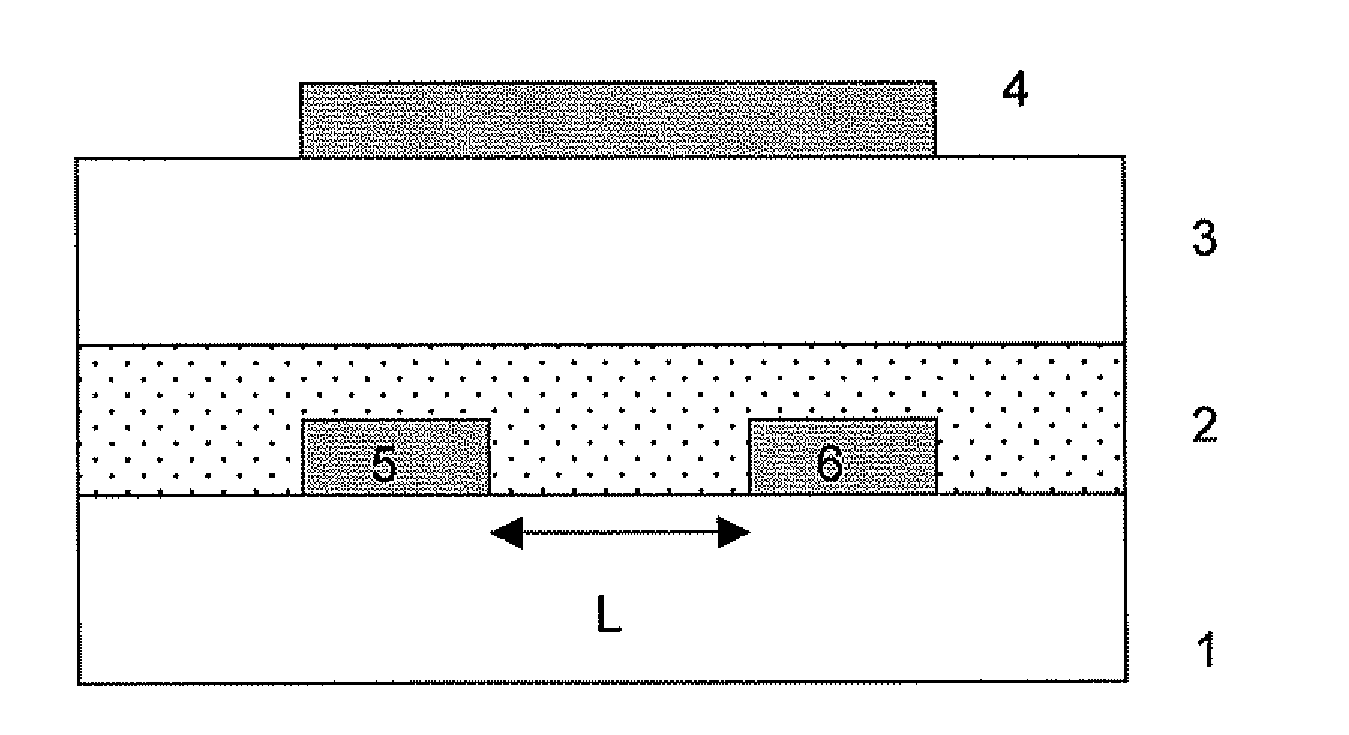
[0168]A test field effect transistor is manufactured by using a glass substrate (Corning Eagle 2000) upon which are patterned Au source and drain electrodes by evaporation though a shadow mask. Following Au source and drain evaporation the samples are cleaned in an oxygen plasma (1 KW, 500 mL / min) for 90 s. The samples are then immersed in 10 mM pentafluorobenzenethiol (Aldrich cat. no. P565-4) for 10 minutes followed by rinsing in 2-propanol and drying under a stream of compressed air.

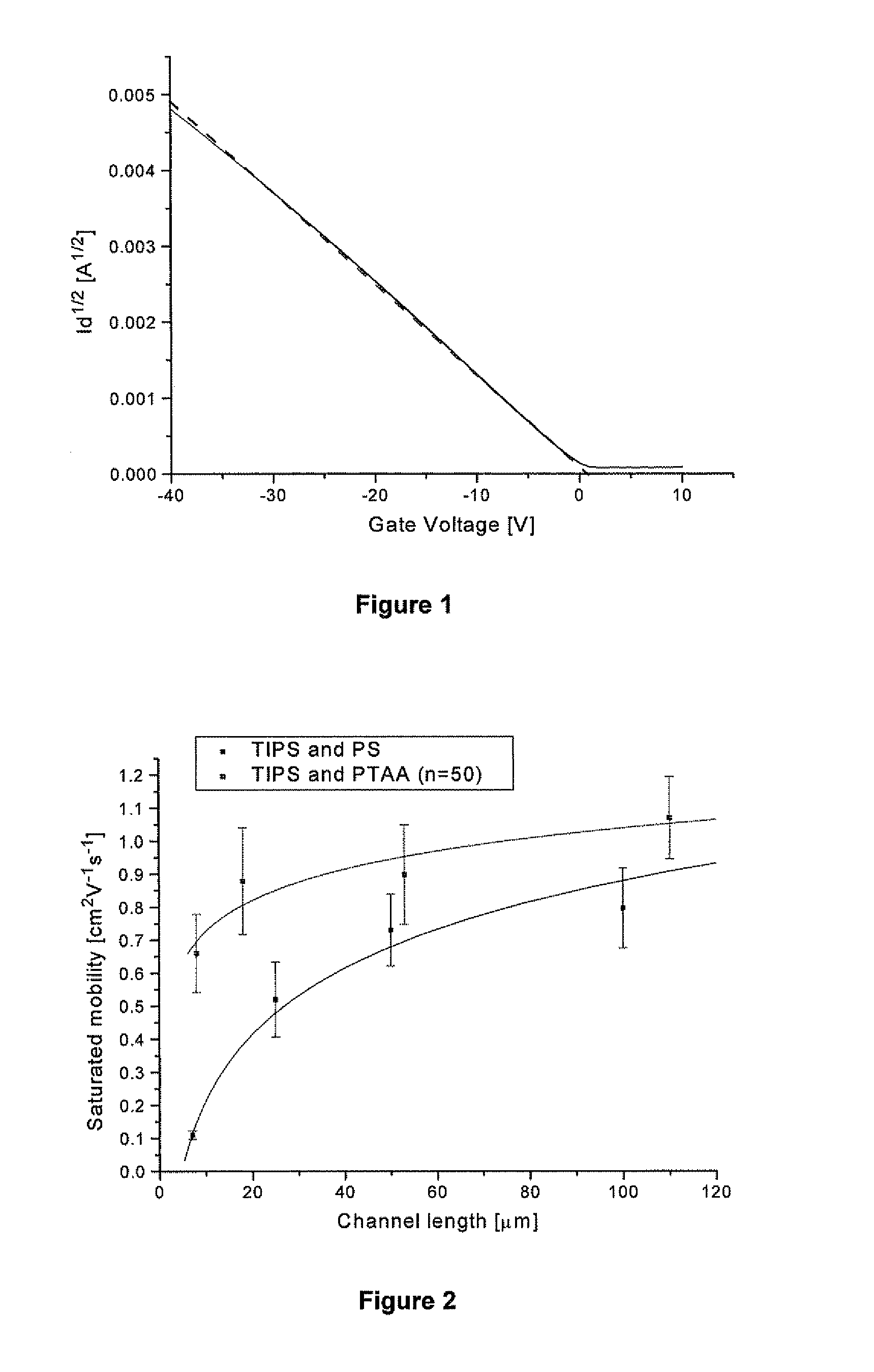
[0169]Semiconductor formulations are made using the OSC compound 6,13-bis(triisopropylsilylethynyl)pentacene (“TIPS”, formula I1 above) blended with PTAA1 (formula II1a above, permittivity 2.9) or an inert binder resin polystyrene (PS Mw 1,000,000 Aldrich cat. no. 48,080-0, permittivity 2.5) (comparative example) at a 1:1 ratio by weight. For the TIPS / PTAA formulation, the semiconductor formulation is dissolved four parts into 96 parts of tetrahydronapthalene, and spin coated onto the substrate at 500...

example 2

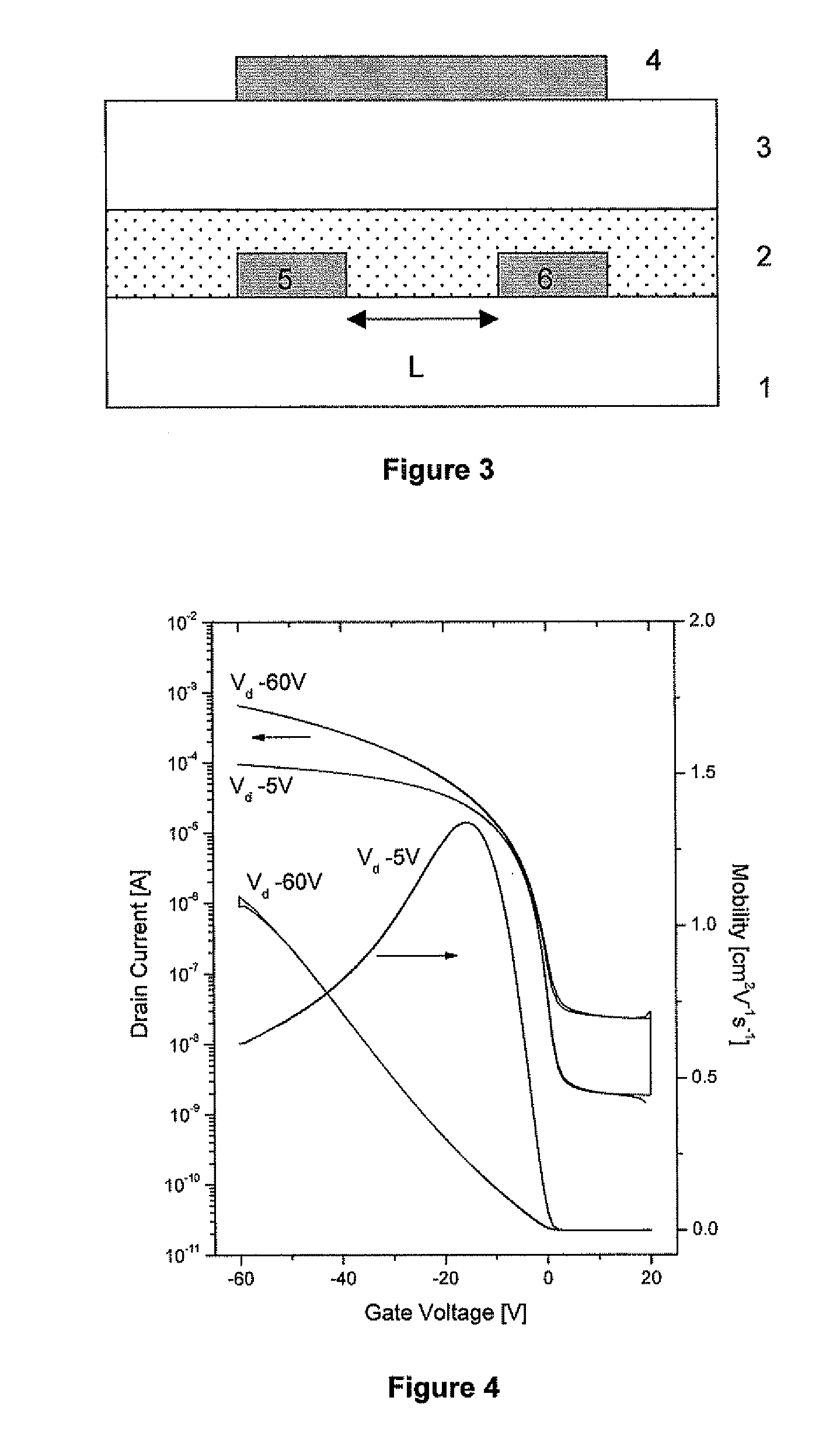
[0175]A test field effect transistor is manufactured using a glass substrate, upon which are patterned Au source and drain electrodes by shadow masking. The electrodes are treated for 1 minute with a 10 mM solution of pentafluorobenzenethiol (Aldrich cat. No. P565-4). A semiconductor formulation is prepared using the compound TIPS (formula I1 above) blended with PTAA1 (formula II1a above, permittivity 2.9) and Spirobifluorene (formula 6 above) in a ratio of 2:1:1 respectively by weight. The semiconductor formulation is dissolved 4 parts into 96 parts of solvent (tetrahydronapthalene), and spin coated onto the substrate and Pt / Pd electrodes at 500 rpm for 20 s followed by 2000 rpm for 20 s. To ensure complete drying the sample is placed on a hotplate for 1 minute at 100° C. followed by 30 minutes in an air oven at 100° C. A solution of the insulator material (Cytop 809M, Asahi glass) is mixed 1:1 by weight with the fluorosolvent FC43 (Acros cat. no.12377) and then spin-coated onto th...


PUM

PropertyMeasurementUnit
channel lengthaaaaaaaaaa
source-drain distanceaaaaaaaaaa

Abstract

The invention relates to an improved electronic device, like an organic field emission transistor (OFET), which has a short source to drain channel length and contains an organic semiconducting formulation comprising a semiconducting binder.

Description

FIELD OF THE INVENTION [0001]The invention relates to an improved electronic device, like an organic field emission transistor (OFET), which has a short source to drain channel length and contains an organic semiconducting formulation comprising a semiconducting binder.BACKGROUND AND PRIOR ART[0002]In recent years, there has been development of organic semiconducting (OSC) materials in order to produce more versatile, lower cost electronic devices. Such materials find application in a wide range of devices or apparatus, including organic field effect transistors (OFETs), organic light emitting diodes (OLEDs), photodetectors, organic photovoltaic (OPV) cells, sensors, memory elements and logic circuits to name just a few. The organic semiconducting materials are typically present in the electronic device in the form of a thin layer, for example less than 1 micron thick.[0003]Improved charge mobility is one goal of new electronic devices. Another goal is improved stability, film unifo...

Claims


Application Information

Patent Timeline
Patent Type & Authority Applications(United States)
IPC IPC(8): H01L51/30H01L51/05H01L51/40H01L51/46H01L51/54
CPCH01L51/0035H01L51/0039H01L51/0055H01L51/105H01L51/0541H01L51/0566H01L51/0094H10K85/111H10K85/115H10K85/623H10K85/40H10K10/488H10K10/464H10K10/84H10K10/80
Inventor OGIER, SIMON DOMINICVERES, JANOSZEIDAN, MUNTHER
Owner MERCK PATENT GMBH
Why Eureka
Try Eureka