Substrate processing method

a substrate and processing method technology, applied in the direction of electrical equipment, basic electric elements, electric discharge tubes, etc., can solve the problems that the minimum pattern dimension produced by photolithography cannot be reduced below a certain limit, and the conventional substrate processing method, however, may not be satisfactory in view of controllability, so as to achieve the effect of improving the effect of etching the bottom portion of the opening and suppressing the deposition of the bottom portion

Inactive Publication Date: 2010-12-09
TOKYO ELECTRON LTD
View PDF39 Cites 7 Cited by
  • Summary
  • Abstract
  • Description
  • Claims
  • Application Information

AI Technical Summary

Benefits of technology

[0042]In the substrate processing method, the anisotropic etching gas may be the CF3I gas, the CF3Br gas, the HI gas or the HBr gas. Therefore, an effec...

Problems solved by technology

Due to non-uniformity in focal lengths, however, the minimum pattern dimension producible by the photolithography cannot be re...

Method used


Image

  • Substrate processing method
  • Substrate processing method
  • Substrate processing method

Examples


experimental examples

[0107]Now, specific experimental examples of the present disclosure will be explained.

experimental example 1

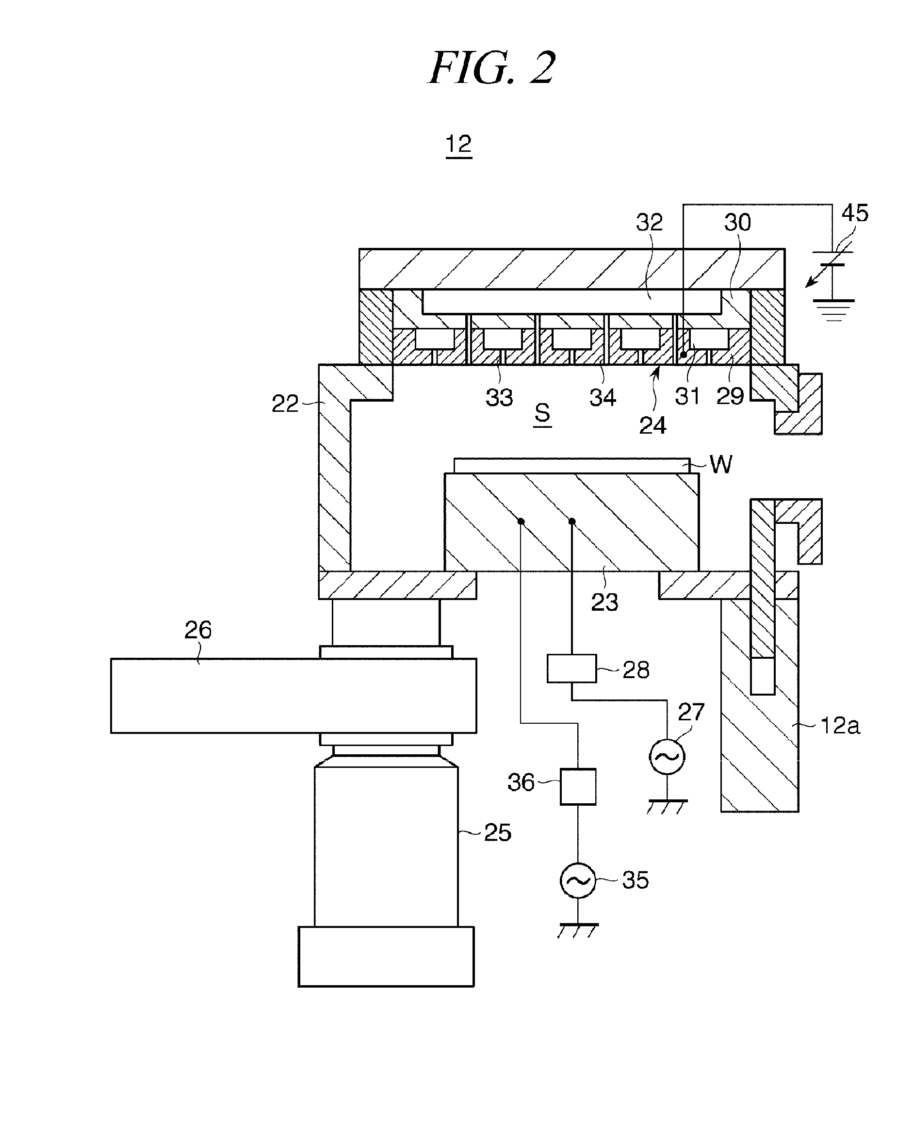
[0108]A plasma etching process was performed on a wafer W of FIG. 3 by using the process module 12 of FIG. 2. As for processing conditions, an internal pressure of the chamber was set to about 2×10 Pa (about 150 mTorr); a temperature of the wafer W, about 60° C.; an excitation power to the mounting table 23, about 750 W; a bias power to the mounting table 23, about 300 W; and a DC voltage to the shower head, about −300 V. Further, a CHF3 gas, a H2 gas, a N2 gas and a CF3I gas are applied as a processing gas at flow rates of about 200 sccm, about 30 sccm, about 30 sccm and about 50 sccm, respectively. CD values of a photoresist film 54 on a wafer W were non-uniform in the range of about 75 nm to about 95 nm before the plasma etching. However, almost uniform openings having CD values ranging from about 31 nm to about 32 nm were formed in a SiON film 52 after the plasma etching.

experimental example 2

[0109]The same plasma etching process as conducted in the experimental example 1 was performed under the same conditions as those of the experimental example 1 excepting that a feed amount of a N2 gas was changed to about 60 sccm. As a result, almost uniform openings having CD values about 18 nm were formed in a SiON film 52.


PUM


Abstract

A substrate processing method performs a processing on a wafer W having an amorphous carbon film 51, a SiON film 52, a BARC film 53 and a photoresist film 54 formed on top of each other in sequence. In the substrate processing method, a shrinking-etching process and a non-uniformity-suppressing process are performed as a single process. The shrinking-etching process etches the SiON film 52 on bottom portions of openings 55 of the photoresist film 54 while reducing CD values of the openings 55 by plasma generated from a gaseous mixture of a CHF3 gas, a CF3I gas, a H2 gas and a N2 gas. The non-uniformity-suppressing process suppresses non-uniformity in the CD values by facilitating deposition of deposits on sidewall surfaces of the openings 55.

Description

CROSS-REFERENCE TO RELATED APPLICATION[0001]This application claims the benefit of Japanese Patent Application No. 2009-136269 filed on Jun. 5, 2009, and U.S. Provisional Patent Application Ser. No. 61 / 222,809 filed on Jul. 2, 2009, the entire disclosures of which are incorporated herein by reference.FIELD OF THE INVENTION[0002]The present disclosure relates to a substrate processing method, and, more particularly, to a substrate processing method for processing a substrate on which a processing target layer, an intermediate layer and a mask layer are formed in sequence.BACKGROUND OF THE INVENTION[0003]For a semiconductor device, there is known a wafer having, on a silicon base, an impurity-containing oxide film such as a TEOS (Tetra Ethyl Ortho Silicate) film formed by a CVD process or the like; a conductive film such as a TiN film; an antireflection film (BARC film); and a photoresist film in sequence (see, for example, Patent Document 1). The photoresist film is formed to have a ...

Claims


Application Information

Patent Timeline
IPC IPC(8): H01L21/3065
CPCH01J37/32091H01L21/31116H01L21/31144H01L21/31138H01L21/31122
Inventor HONDA, MASANOBU
Owner TOKYO ELECTRON LTD
Why Eureka
Try Eureka