

Data processing apparatus and method for performing a predetermined rearrangement operation
a data processing apparatus and predetermined technology, applied in the field of predetermined rearrangement operation, can solve the problems of increasing the complexity of the register bank, and affecting the operation efficiency of the data processing apparatus
- Summary
- Abstract
- Description
- Claims
- Application Information
AI Technical Summary
Benefits of technology
Problems solved by technology
Method used
Image

Examples
Embodiment Construction
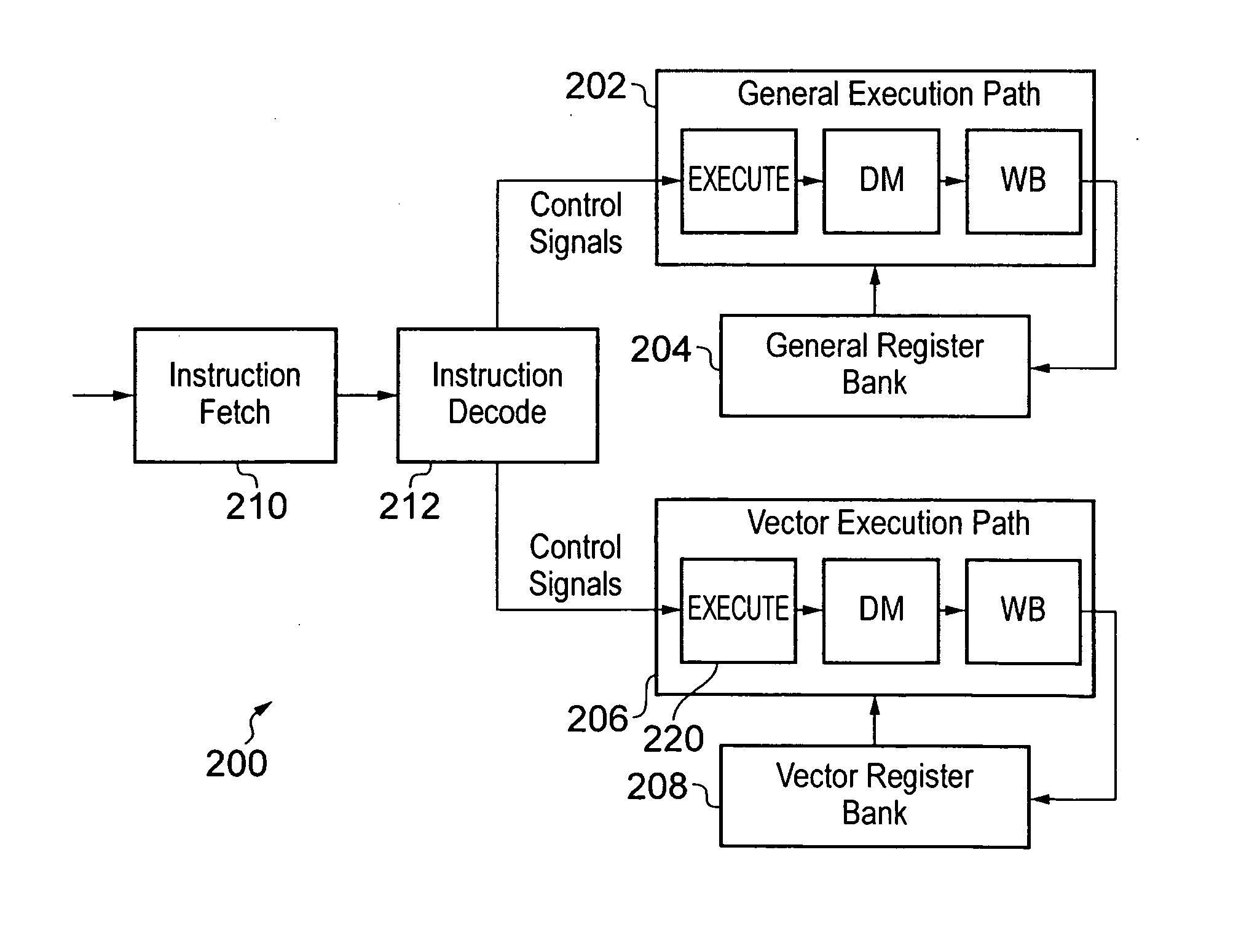
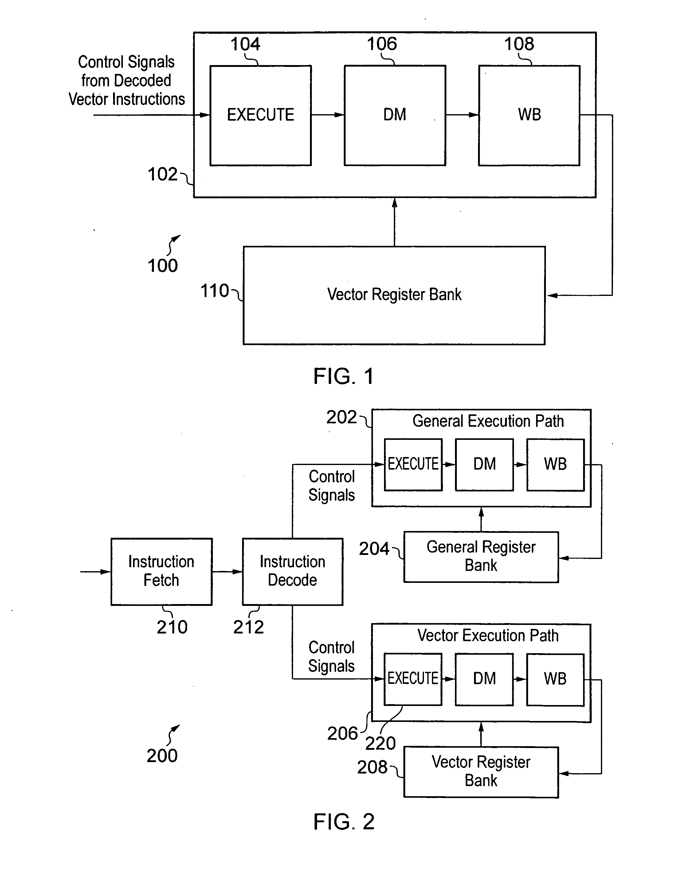
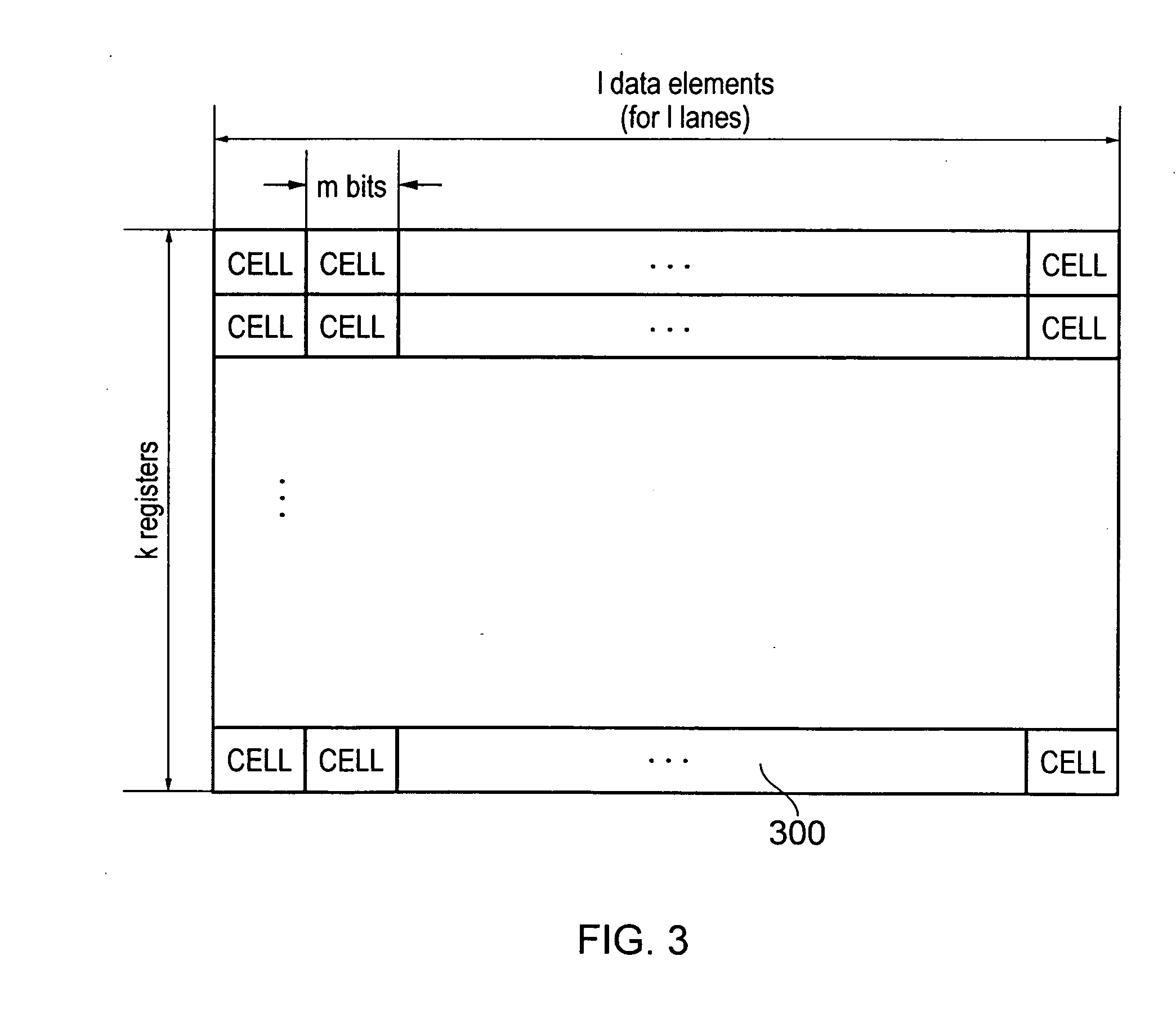
[0053]FIG. 1 schematically illustrates at least a part of a processor 100 according to an embodiment. The processor 100 comprises a dedicated vector processing unit (also referred to herein as a vector execution unit) 102 to which the control signals from decoded vector instructions are fed. The processor 100 is preferably a pipelined processor, where the dedicated vector execution unit 102 can comprise stages for arithmetic logical operations 104, data memory access 106, and register write back 108. Associated with the dedicated vector execution unit 102, there is provided a vector register bank 110 comprising a first number k of vector registers each comprising a second number 1 of data elements where each data element has a third number m of bits, for example as illustrated in FIG. 3. The vector processing unit comprises a plurality of lanes of parallel processing, and in one embodiment, when executing a vector instruction specifying one or more input vector registers, each lane ...
PUM
 Abstract
Description
Claims
Application Information