
Ultra-Low Dislocation Density Group III - Nitride Semiconductor Substrates Grown Via Nano- Or Micro-Particle Film

a technology of nitride and semiconductor substrates, which is applied in the direction of polycrystalline material growth, crystal growth process, chemically reactive gas, etc., can solve the problems of easy influence of growth layer, easy to match low lattice constant to substrate crystal lattice constant, and accumulate elastic bending energy

Inactive Publication Date: 2010-12-23
NANOCRYSTAL CORP
View PDF5 Cites 50 Cited by
  • Summary
  • Abstract
  • Description
  • Claims
  • Application Information

AI Technical Summary

Problems solved by technology

This very low lattice constant is very difficult to match to the lattice constant of a substrate crystal (such as sapphire, silicon, silicon carbide, gallium arsenide etc).
Generally, if the lattice constant of a substrate crystal differs from the lattice constant of a crystal to be epitaxially grown on the substrate crystal, the resulting growth layer is easily affected by a compressive bending or tensile bending and tends to disadvantageously accumulate an elastic bending energy therein.
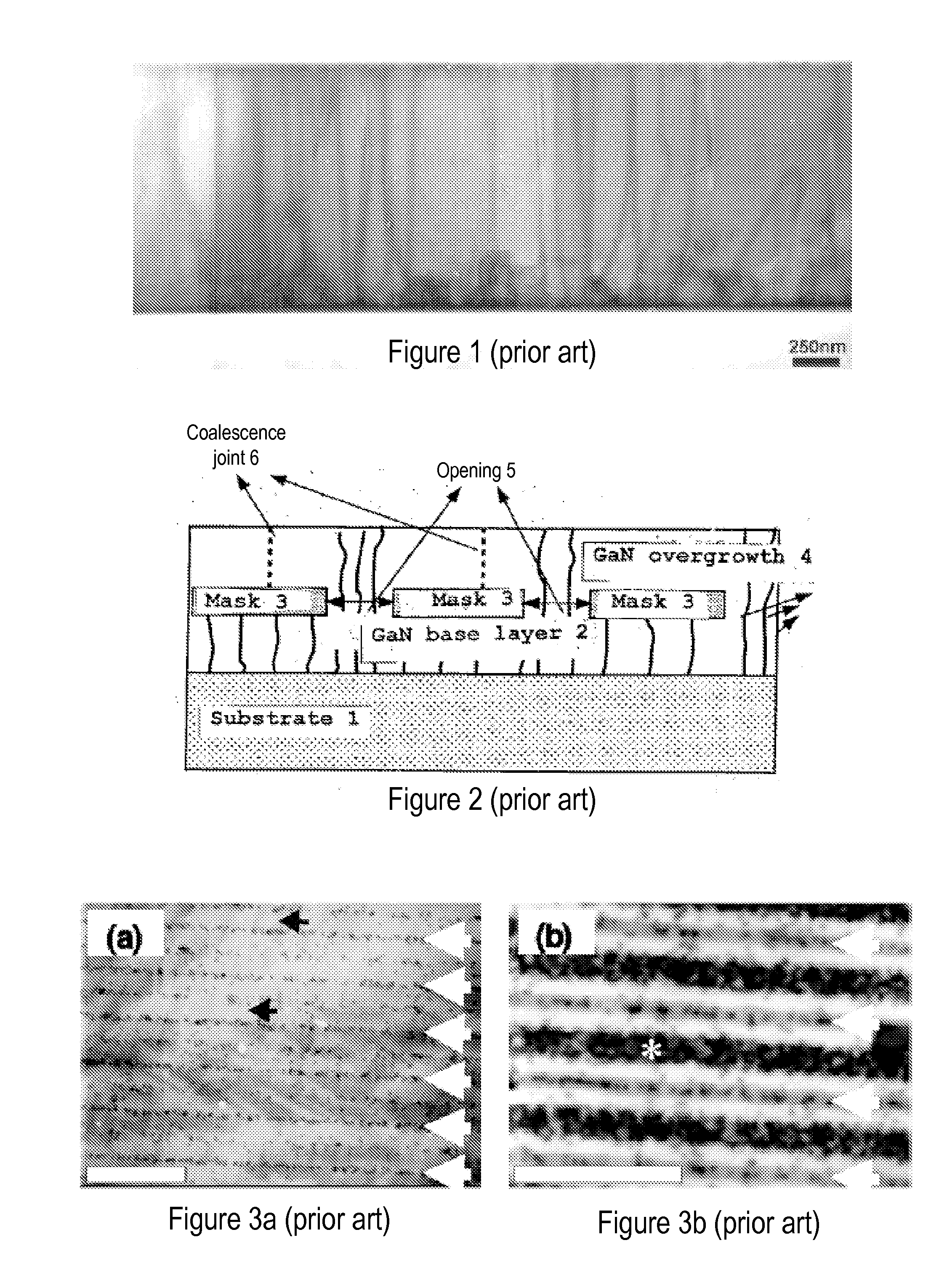
Although this elastic energy is within an allowable range if the growth layer is thin, the elastic energy may generate an electric potential if the thickness of the growth layer exceeds a certain critical value, thus causing lattice relaxation and resulting in a great amount of electric defects and dislocations in the growth layer, as shown in FIG. 1.
These dislocations are harmful in several respects.
Firstly, at a high density (i.e., higher than 1×107 cm−2), dislocations degrade electronic mobility and electronic properties (photoluminescence intensity, life of carriers).
Furthermore, the emergence of surface dislocations results in surface depression.
In a laser diode structure based on InGaN multi-quantum wells (MQWs), the dislocations may disturb the order of MQWs and cause non-homogeneous light emission.
Consequently, it is impossible to use the entire surface to manufacture optoelectronic components using a conventional ELO process.
Therefore, the manufacturing technology for a laser diode on an ELO substrate as described above requires a complex technology because the diode structure needs to be made on overgrowth zones 4, between the coalescence joint and the zone in epitaxial contact with the substrate.
This requires an alignment precision on the order of 1 micrometer (μm), which results in a complicated, low-yield and high-cost process.
Even though the two-step ELO results in improved wafer quality compared to one step ELO, it is also significantly more expensive since it requires two patterning and three epitaxial growth steps.

Method used


Image

  • Ultra-Low Dislocation Density Group III - Nitride Semiconductor Substrates Grown Via Nano- Or Micro-Particle Film
  • Ultra-Low Dislocation Density Group III - Nitride Semiconductor Substrates Grown Via Nano- Or Micro-Particle Film
  • Ultra-Low Dislocation Density Group III - Nitride Semiconductor Substrates Grown Via Nano- Or Micro-Particle Film

Examples


Embodiment Construction

[0027]Objectives and advantages of the invention may be obvious from the foregoing description, will be set forth in part in the description that follows, or may be learned by practice of the invention. It is to be understood that both the foregoing description and the following description are exemplary and explanatory only and are not restrictive of the invention, as claimed. The objectives and advantages of the invention will be realized and attained by means of the elements and combinations particularly pointed out in the appended claims. Various embodiments may achieve some, all or none of the following objectives.

[0028]One desirable objective is to provide an ultra low defect or dislocation density Group III-Nitride semiconductor crystal in which the strain with the starting substrate is more relaxed and crystal defect or dislocation density is lower than conventional methods, and having characteristics that are generally uniform across the surface of the substrate. The growth...


PUM


Abstract

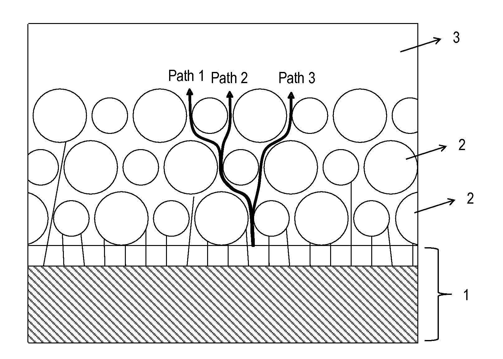
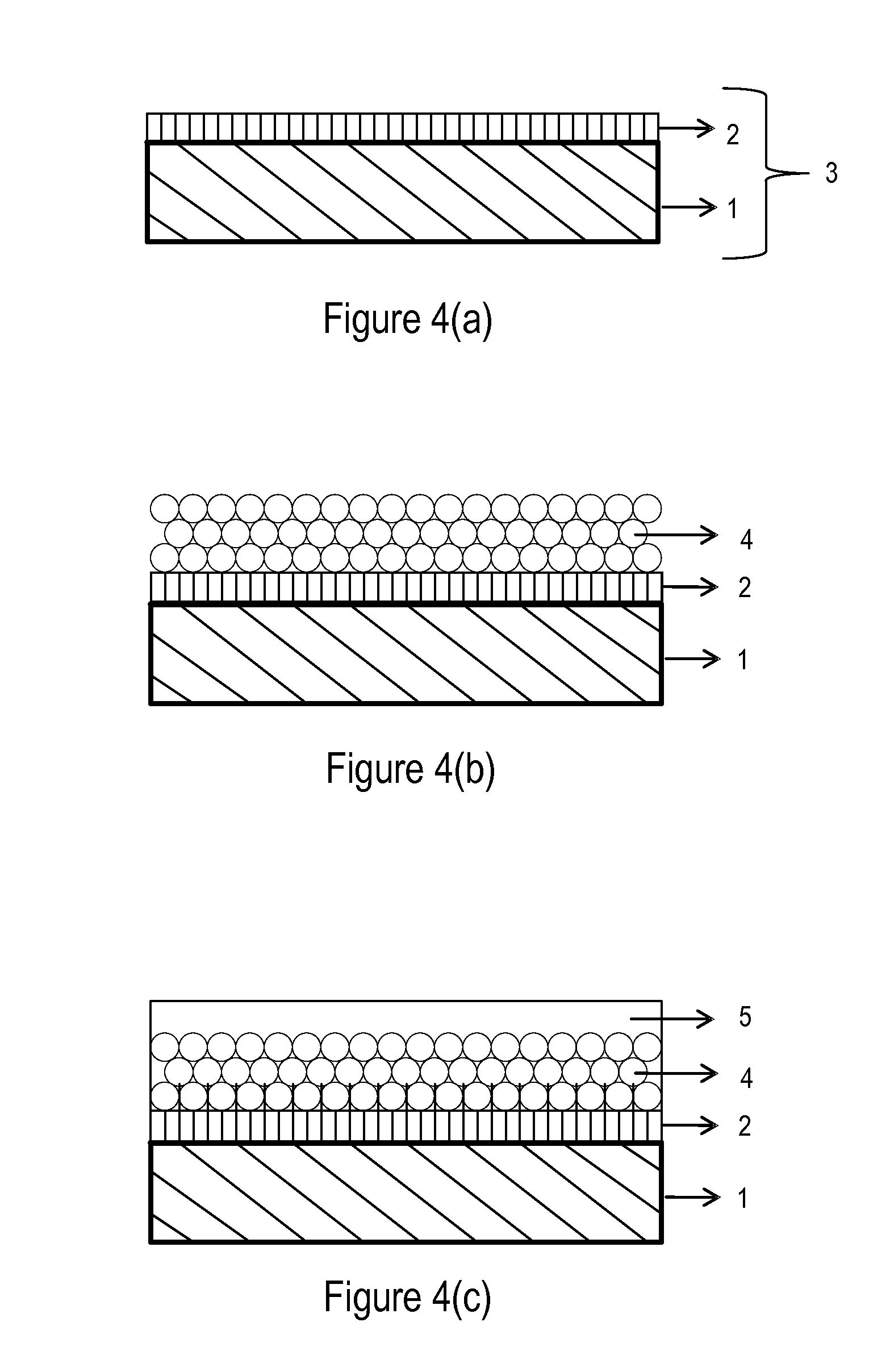
A high quality Group III-Nitride semiconductor crystal with ultra-low dislocation density is grown epitaxially on a substrate via a particle film with multiple vertically-arranged layers of spheres with innumerable micro- and / or nano-voids formed among the spheres. The spheres can be composed of a variety of materials, and in particular silica or silicon dioxide (SiO2).

Description

CROSS-REFERENCE TO RELATED APPLICATION(S)[0001]This application claims priority under 35 U.S.C. §119(e) to U.S. Provisional Patent Application Ser. No. 61 / 004,485, “Manufacturing of Ultra-Low Dislocation Density Group III-Nitride Semiconductor Substrate Based on Epitaxial Growth via Particle Film with Micro-voids,” filed Nov. 27, 2007; Ser. No. 61 / 007,785, “Manufacturing of Ultra-Low Dislocation Density Group III-Nitride Semiconductor Substrate Based on Epitaxial Growth via Particle Film with Micro- or Nano-Spheres,” filed Dec. 13, 2007; and Ser. No. 61 / 021,596, “Ultra-Low Dislocation Density Group III-Nitride Semiconductor Substrates Grown Via Nano- or Micro-Particle Film,” filed Jan. 16, 2008. The subject matter of all of the foregoing is incorporated herein by reference in their entirety.BACKGROUND OF THE INVENTION[0002]1. Field of the Invention[0003]The present invention relates to a high quality Group III-Nitride semiconductor crystal with ultra-low dislocation density grown ep...

Claims


Application Information

Patent Timeline
IPC IPC(8): H01L29/06H01L21/04H01L29/12
CPCC30B23/02H01L21/02642C30B25/02C30B25/18C30B29/403C30B29/406H01L21/0237H01L21/02378H01L21/02381H01L21/0242H01L21/02458H01L21/0254H01L21/0262H01L21/02631H01L21/02639C30B23/025
Inventor VARANGIS, PETROS M.ZHANG, LEI
Owner NANOCRYSTAL CORP
Learn More