
Fabrication method of gallium nitride-based compound semiconductor

a technology of gallium nitride and compound semiconductor, which is applied in the direction of semiconductor devices, basic electric elements, electrical equipment, etc., can solve the problems of relatively high defect density, low manufacturing cost effectiveness, and inability to achieve large-sized substrates for mass production, so as to improve the crystal quality of a continuously growing gan-based semiconductor layer, improve the crystal quality, and improve the effect of crystal quality

Inactive Publication Date: 2011-01-06
SINO AMERICAN SILICON PROD
View PDF13 Cites 17 Cited by
  • Summary
  • Abstract
  • Description
  • Claims
  • Application Information

AI Technical Summary

Benefits of technology

[0011]It is a primary objective of the present invention to provide a fabrication method of a GaN-based compound semiconductor, particularly a fabrication method of forming and superimposing the wetting layer on a ZnO-based semiconductor layer and nitrifying the wetting layer many times to form a transition layer, so as to improve the crystal quality of a continuously growed GaN-based semiconductor layer.
[0012]Another objective of the present invention is to provide a fabrication method of GaN-based compound semiconductor, particularly a fabrication method of forming a wetting layer on a ZnO-based semiconductor layer at the first temperature, and then nitrifying the wetting layer at the second temperature many times to form a transition layer, so as to improve the crystal quality of the GaN-based semiconductor layer, wherein the second temperature is not less than the first temperature.
[0013]A further objective of the present invention is to provide a fabrication method of a GaN-based compound semiconductor, particularly a fabrication method of forming a first transition layer on a ZnO-based semiconductor layer at a first temperature, and then forming a second transition layer at a second temperature, so as to improve the crystal quality of the continuously grown GaN-based semiconductor layer, wherein the temperature of forming the second transition layer is no less than the temperature of forming the first transition layer.
[0014]Another objective of the present invention is to provide a fabrication method of a GaN-based compound semiconductor, particularly a fabrication method of forming and superimposing different wetting layers on a ZnO-based semiconductor layer and nitrifying the wetting layers many times to form a transition layer, so as to improve the crystal quality of the continuously grown GaN-based semiconductor layer.
[0015]Another objective of the present invention is to provide a fabrication method of GaN-based compound semiconductor, particularly a fabrication method of forming a transition layer by the steps of forming a wetting layer on a ZnO-based semiconductor layer and nitrifying the wetting layer, and the transition layer not only protects the surface of the ZnO-based semiconductor layer, but also provides a buffer layer to improve the crystal quality of a continuously grown GaN-based semiconductor layer.

Problems solved by technology

However, due to the technical bottleneck of directly forming a bulk GaN compound semiconductor still cannot be overcome, and thus, the large-sized substrate cannot be achieved for mass productions to lower the manufacturing cost effectively.
Although the conventional way of using sapphire or silicon carbide as a substrate to grow a GaN-based layer is used extensively and commercialized, yet the issue of lattice mismatch between the aforementioned substrates and GaN-based layer still exists, and thus the GaN-based layer fabricated by the conventional method still has a relatively high defect density which will cause the light emission efficiency and electron mobility unable to be enhanced in the applications of light emitting devices specially.
Therefore, the conventional method has some drawbacks.
However, this method has the drawback of incurring a higher cost.
Although this patented technology may reduce the defect density below 1×108 cm−2 by a thinner epitaxial layer, yet it cannot be easily controlled about the uniformity and the density of patterns on a sapphire surface, and thus the yield rate is difficult to control.

Method used


Image

  • Fabrication method of gallium nitride-based compound semiconductor
  • Fabrication method of gallium nitride-based compound semiconductor
  • Fabrication method of gallium nitride-based compound semiconductor

Examples


Embodiment Construction

[0028]The technical measures taken for achieving the aforementioned objectives, and the effects, structures and characteristics of the present invention will become apparent in the following detailed description with reference to the accompanying drawings.

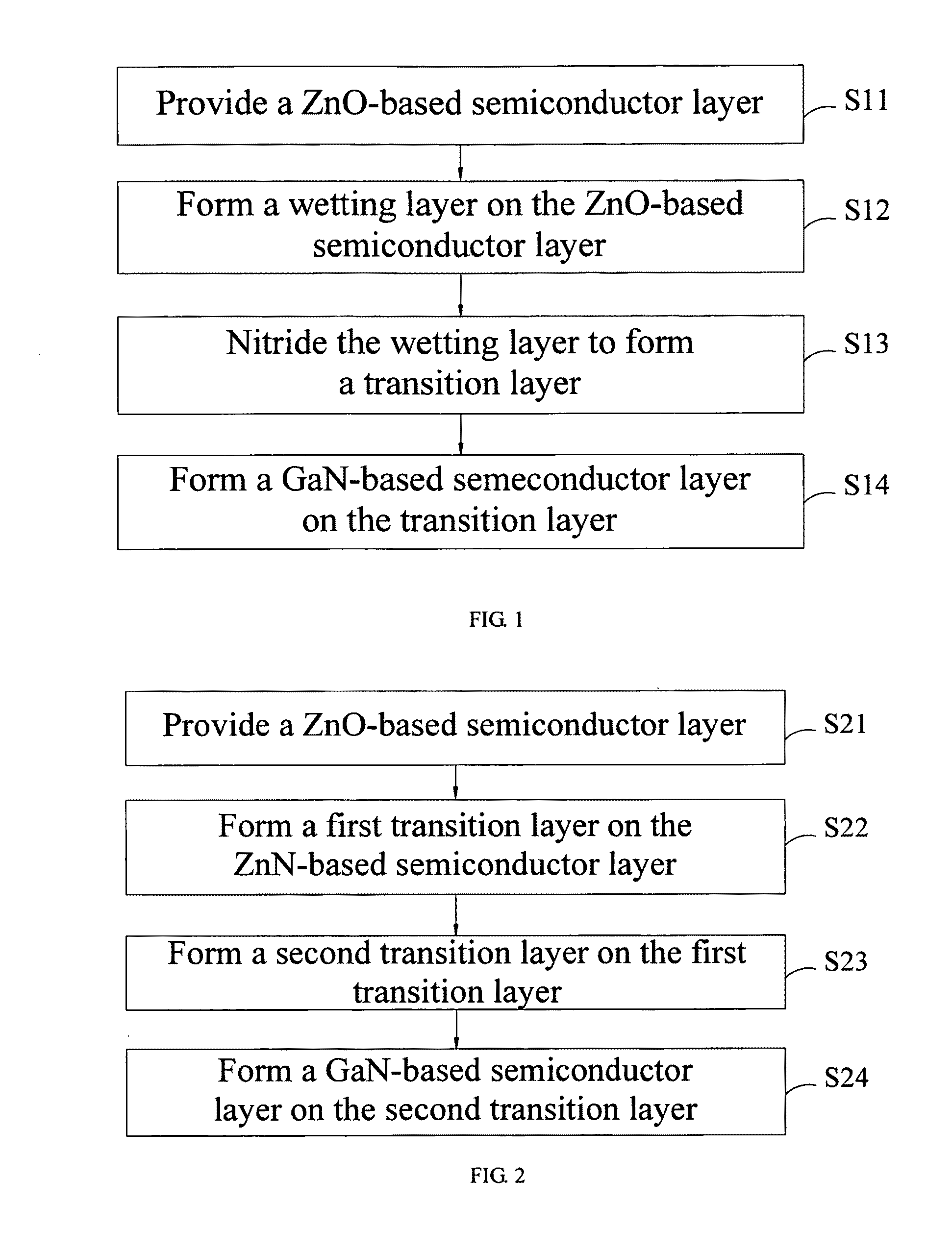
[0029]With reference to FIG. 1 for a flow chart of a fabrication method in accordance with the present invention, the fabrication method comprises the following steps:

[0030]Step S11: Provide a ZnO-based semiconductor layer;

[0031]Step S12: Form a wetting layer on the ZnO-based semiconductor layer;

[0032]Step S13: Nitrify the wetting layer to form a transition layer; and

[0033]Step S14: Form a GaN-based semiconductor layer on the transition layer.

[0034]Wherein, Step S11 further comprises the steps of forming a ZnO-based semiconductor layer on a different substrate, and then repeating Steps S12 and S13 to form and superimpose a wetting layer and nitrify the wetting layer for many times, and Step S14 further comprises many stages with di...


PUM


Abstract

The present invention discloses a method for fabricating gallium nitride(GaN)-based compound semiconductors. Particularly, this invention relates to a method of forming a transition layer on a zinc oxide (ZnO)-based semiconductor layer by the steps of forming a wetting layer and making the wetting layer nitridation. The method not only provides a function of protecting the ZnO-based semiconductor layer, but also uses the transition layer as a buffer layer for a following epitaxial growth of a GaN-based semiconductor layer, and thus, the invention may improve the crystal quality of the GaN-based semiconductor layer effectively.

Description

BACKGROUND OF THE INVENTION[0001]1. Field of the Invention[0002]The present invention relates to a method for fabricating GaN-based compound semiconductor, in particular to a fabrication method that inserts a transition layer between a GaN-based semiconductor layer and a ZnO-based semiconductor layer to improve the crystal quality of the GaN-based semiconductor layer.[0003]2. Description of the Related Art[0004]Currently, according to the available light emitting devices, the GaN-based semiconductor material is a very important wide bandgap material which is applied to red, blue, and ultraviolet light emitting devices. However, due to the technical bottleneck of directly forming a bulk GaN compound semiconductor still cannot be overcome, and thus, the large-sized substrate cannot be achieved for mass productions to lower the manufacturing cost effectively. Although the conventional way of using sapphire or silicon carbide as a substrate to grow a GaN-based layer is used extensively ...

Claims


Application Information

Patent Timeline
IPC IPC(8): H01L21/20H01L33/00
CPCH01L21/0237H01L21/02403H01L21/0242H01L21/0243H01L21/02458H01L33/12H01L21/02507H01L21/0254H01L21/0262H01L33/007H01L21/02472
Inventor CHEN, MIIN-JANGYU, SHENG-FULIN, RAY-MINGHSU, WEN-CHINGHO, SZU-HUA
Owner SINO AMERICAN SILICON PROD
Learn More