Methods of manufacture of vertical nanowire fet devices

Active Publication Date: 2011-01-20
GLOBALFOUNDRIES US INC
View PDF26 Cites 148 Cited by
  • Summary
  • Abstract
  • Description
  • Claims
  • Application Information

AI Technical Summary

Benefits of technology

[0018]It is still another object of this invention to improve the controllability and flexibility of the method of fabricating electroplated nanowire based FETs.
[0019]It is also desir

Problems solved by technology

However, because of fundamental scaling limits, advanced FETs rely increasingly on nontraditional materials and structures and special integration schemes to achieve desired improvements in circuit performance.
Furthermore, the integration of vertical FETs in a three dimensional fashion has been another nontraditional method to improve the device performance at the system level.
The performance of the devices becomes hard to control as a result of the variation in the nanowire diameter.
The devices described therein generally suffer from the poor controllability of the processes.
A FET fabricated using the process in the

Method used


Image

  • Methods of manufacture of vertical nanowire fet devices
  • Methods of manufacture of vertical nanowire fet devices
  • Methods of manufacture of vertical nanowire fet devices

Examples


first embodiment

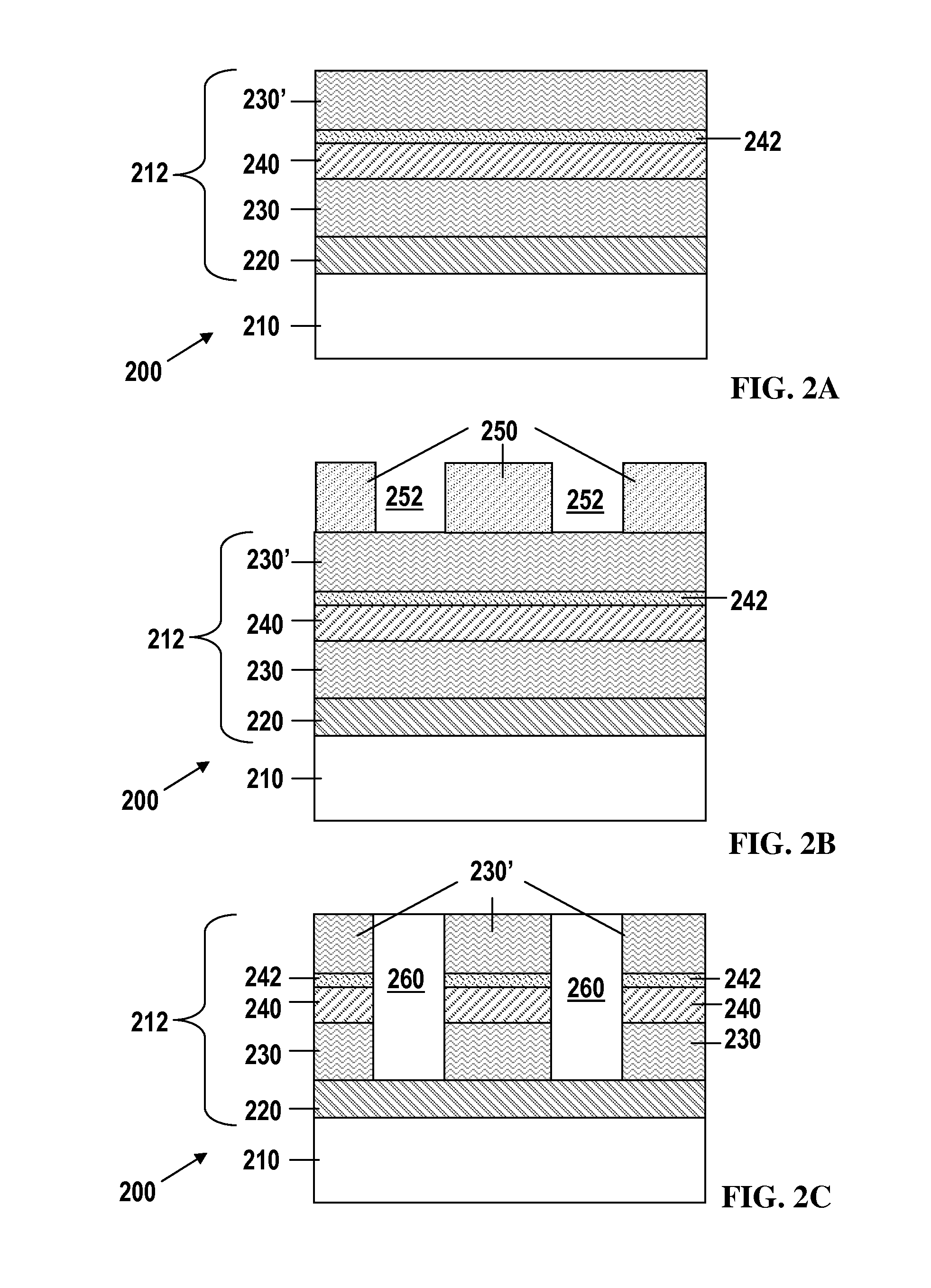
[0040]FIGS. 2A to 2H are schematic diagrams showing processing steps of a method for fabrication of a vertical Field Effect Transistor (FETS) FETs 200 with electroplated semiconductor nanowires as the device channels according to one embodiment of the present invention.

[0041]FIG. 2A shows a vertical FET 200 in accordance with this invention in an early stage of fabrication thereof consisting of a stack 212 of layers formed on a substrate 210. The stack 212 of layers comprises a conductive layer 220, a spacer layer 230, a gate electrode layer 240, and a second spacer layer 230′. The substrate 210 can be composed of any nonconductive, or highly resistive semiconductor material, including but not limited to aluminum oxide, magnesium oxide, zinc oxide, silicon oxide, silicon nitride, glass, undoped silicon, silicon carbide, and combinations thereof.

[0042]The substrate 210 can also comprise a layered structure with a top surface being nonconductive or highly resistive. The conductive lay...

second embodiment

[0059]FIGS. 3A to 3H are schematic diagrams showing a method of fabricating a vertical FET with electroplated semiconductor nanowires according to another embodiment of the present invention.

[0060]FIG. 3A shows a substrate structure 300 in accordance with this invention in an early stage of fabrication thereof consisting of a substrate 310 with a stack 312 of layers formed thereon. The substrate 310 can be composed of a material that is suitable for the substrate 210 in FIG. 2A. The stack of layers comprises layers of conductive layer 320, spacer layer 330, and sacrificial layer 340. The conductive layer 320 is to be formed into the source or drain electrode. The conductive layer 320 and the spacer layer 330 can be composed of any material that is suitable respectively for the bottom conductive layer 220 and the spacer layer 230 as described with reference to FIG. 2A. The sacrificial layer 340 can be composed of any material that can be removed selectively later composed of a materi...

third embodiment

[0069]FIGS. 4A to 4H are schematic diagrams showing a further alternative method of fabricating a vertical FET with electroplated semiconductor nanowires according to a third embodiment of the present invention.

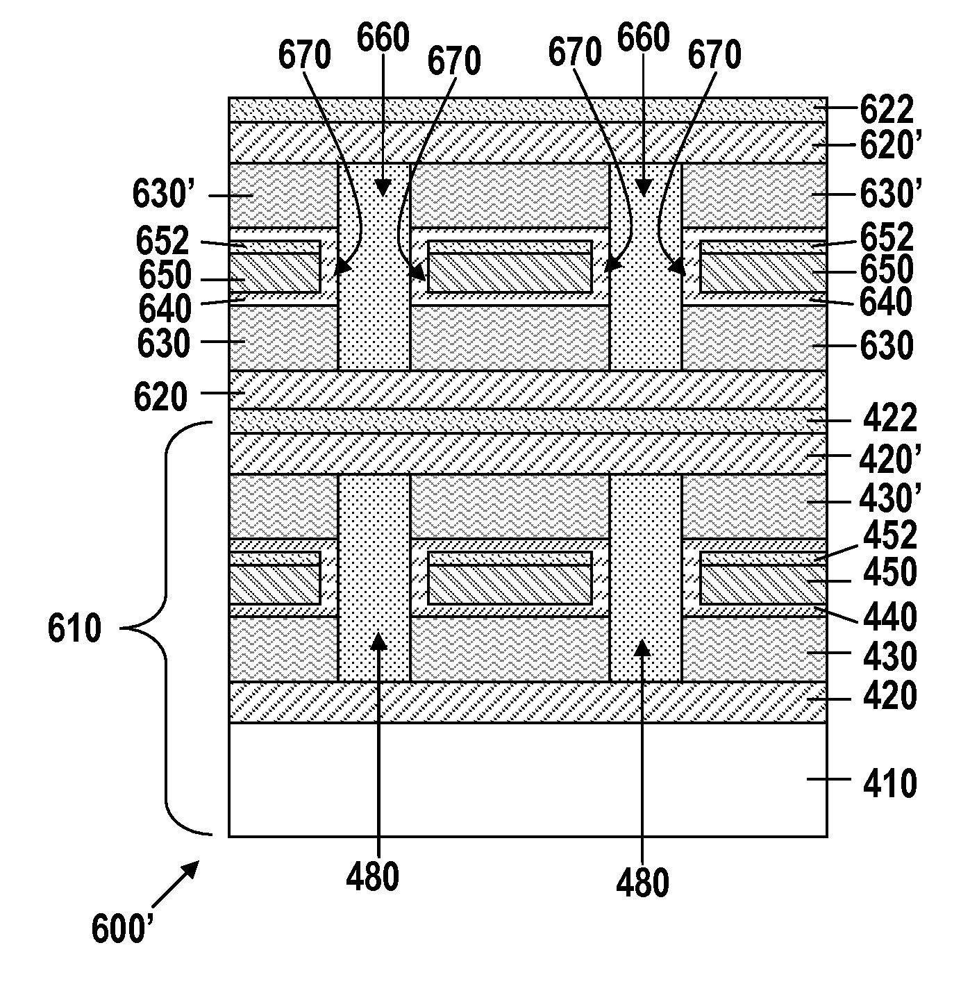
[0070]FIG. 4A shows a substrate structure 400 consisting of a substrate 410 and a stack 412 of layers on the substrate 410. The stack of layers comprises a conductive layer 420, a spacer layer 430, and a gate electrode layer 450 and an optional capping layer 452 on top to protect the gate electrode layer 450 from being damaged in subsequent processing. Between the spacer layer 430 and the gate electrode layer 450, the stack can also have an optional gate dielectric layer 440. The substrate 410 can be composed of any material that is suitable for the substrate 210 in FIG. 2A. The conductive layer 420 serves as the source or drain electrode and it can be composed of any material that is suitable for the bottom conductive layer 220 in FIG. 2A. The spacer layer 430 can be compose...


PUM


Abstract

A vertical Field Effect Transistor (FET) comprising a vertical semiconductor nanowire is formed by the following steps. Create a columnar pore in a bottom dielectric layer formed on a bottom electrode. Fill the columnar pore by plating a vertical semiconductor nanowire having a bottom end contacting the bottom electrode. The semiconductor nanowire forms an FET device with a FET channel region between a source region and a drain region formed in distal ends of the vertical semiconductor nanowire. Form a gate dielectric layer around the channel region of the vertical semiconductor nanowire and then form a gate electrode around the gate dielectric layer. Form a top electrode contacting a top end of the vertical semiconductor nanowire.

Description

CROSS-REFERENCE TO RELATED APPLICATIONS[0001]The present application is related to copending U.S. patent application Ser. No. 11 / 620,224 filed 5 Jan. 2007 of S. W. Bedell et al. entitled “Structures Containing Electrodeposited Germanium and Methods for Their Fabrication” (Attorney Docket No. YOR200600444US1) and copending U.S. patent application Ser. No. 11 / 620,391 filed 5 Jan. 2007 of H. Deligianni et al. entitled “Self-Constrained Anisotropic Germanium Nanostructure from Electroplating” (Attorney Docket No. YOR200600385US1), which were assigned to International Business Machines Corporation, the assignee of the present application. The contents of the above two patent applications is incorporated herein by reference for all purposes.BACKGROUND OF THE INVENTION[0002]The present invention relates to Field Effect Transistor (FET) devices formed of semiconductor nanowires and to a method to fabrication thereof. More particularly, the present invention relates to vertical FET devices w...

Claims


Application Information

Patent Timeline
IPC IPC(8): H01L29/775H01L21/336
CPCB82Y10/00H01L21/02521H01L21/02628H01L21/02639H01L29/78642H01L29/0676H01L29/42392H01L29/66742H01L29/775H01L29/0665
Inventor DELIGIANNI, HARIKLIAHUANG, QIANGROMANKIW, LUBOMYR T.
Owner GLOBALFOUNDRIES US INC
Why Eureka
Try Eureka