Surface emitting laser, surface emitting laser array, and optical apparatus

a laser array and surface technology, applied in the direction of laser optical resonator construction, laser details, semiconductor lasers, etc., can solve the problems of large strain, large difference in refractive index, and limited material content of multilayer film semiconductors, so as to suppress degradation of basic characteristics of elements and prevent heat resistance. , the effect of increasing the heat resistan

Inactive Publication Date: 2011-02-03
CANON KK
View PDF5 Cites 11 Cited by
  • Summary
  • Abstract
  • Description
  • Claims
  • Application Information

AI Technical Summary

Benefits of technology

[0039]In consideration of the above-described problems, the present invention provides a surface emitting laser, a surface emitting laser array, and an optical apparatus, in which an occurrence of warping of a substrate is eliminated or at least minimized by using a quaternary or higher material. In addition, a significant increase in heat resistance can be prevented, so as to suppress degradation of basic characteristics of an element due to heat.
[0045]According to the present invention, a surface emitting laser, a surface emitting laser array, and an optical apparatus can be realized, wherein an occurrence of warping of a substrate is eliminated by using a quaternary or higher material and, in addition, a significant increase in heat resistance can be prevented, so as to suppress degradation of basic characteristics of an element due to heat.

Problems solved by technology

However, it is necessary that a single-crystal layer is produced by growing a crystal and, therefore, materials for constituent layers of the multilayer film semiconductor are limited to materials with lattice match to the substrate.
Furthermore, regarding the use of semiconductor materials and combinations thereof with the above-described lattice match, a large value of difference in refractive index is not obtained as compared with the case in which dielectrics are used.
Therefore, even if each strain is at a low level, a total thickness of layers having the strain becomes very large and, thereby, accumulation of the strain exerts a large effect.
Moreover, it is significantly feared that internal presence of accumulated strain exerts an influence on the reliability.
Consequently, an element formed by using a quaternary or higher material has problems in that the heat resistance becomes large, heat dissipation is small, the internal temperature of the element is raised and, along with that, the element characteristics are degraded.
In particular, regarding a red surface emitting laser having a poor temperature characteristic, an increase in heat resistance leads to significant degradation of the element characteristics, so that even if the problems due to the accumulated strain can be solved, intrinsic requirements concerning the element characteristics are not satisfied.

Method used


Image

  • Surface emitting laser, surface emitting laser array, and optical apparatus
  • Surface emitting laser, surface emitting laser array, and optical apparatus
  • Surface emitting laser, surface emitting laser array, and optical apparatus

Examples


example 1

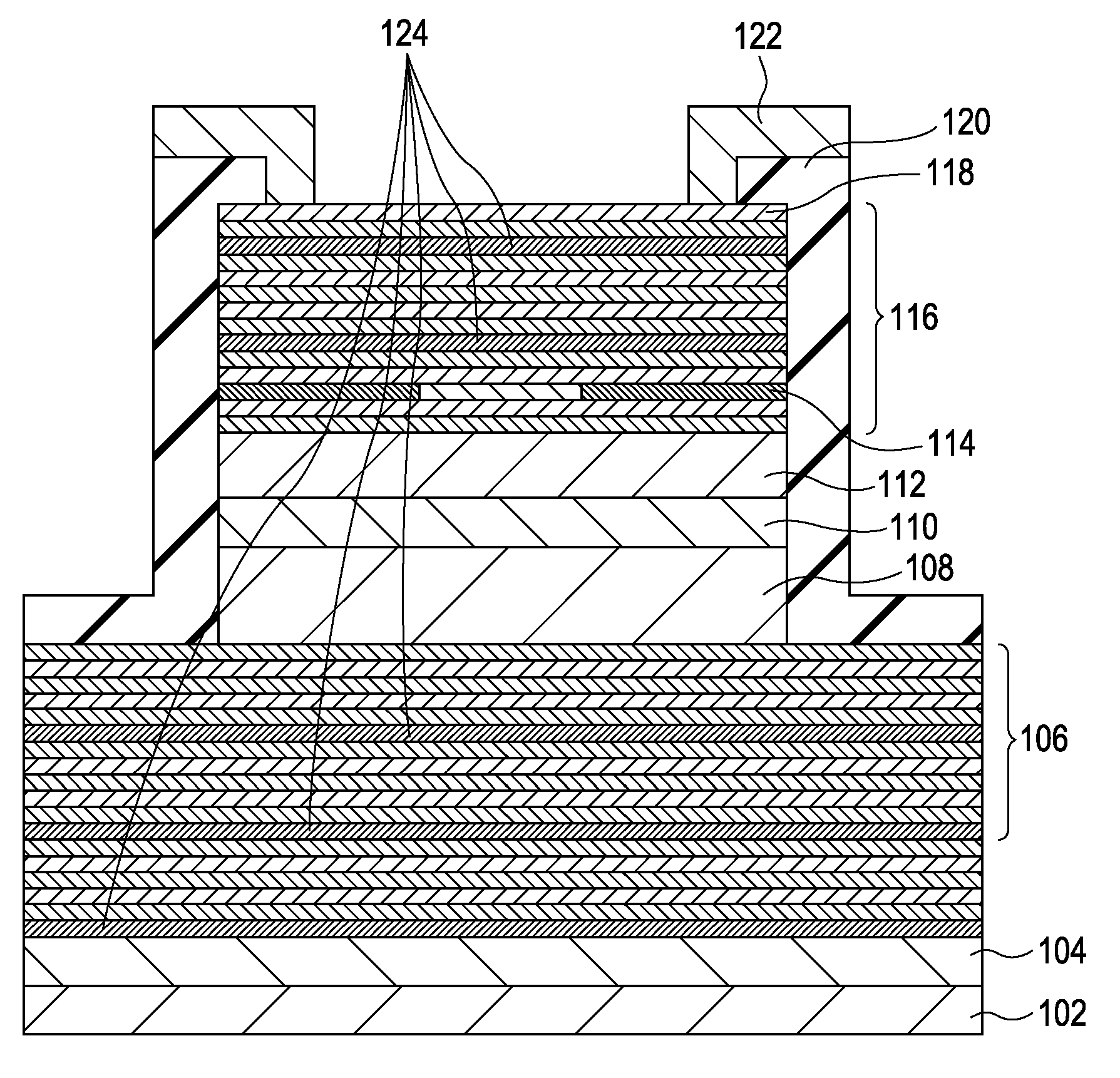
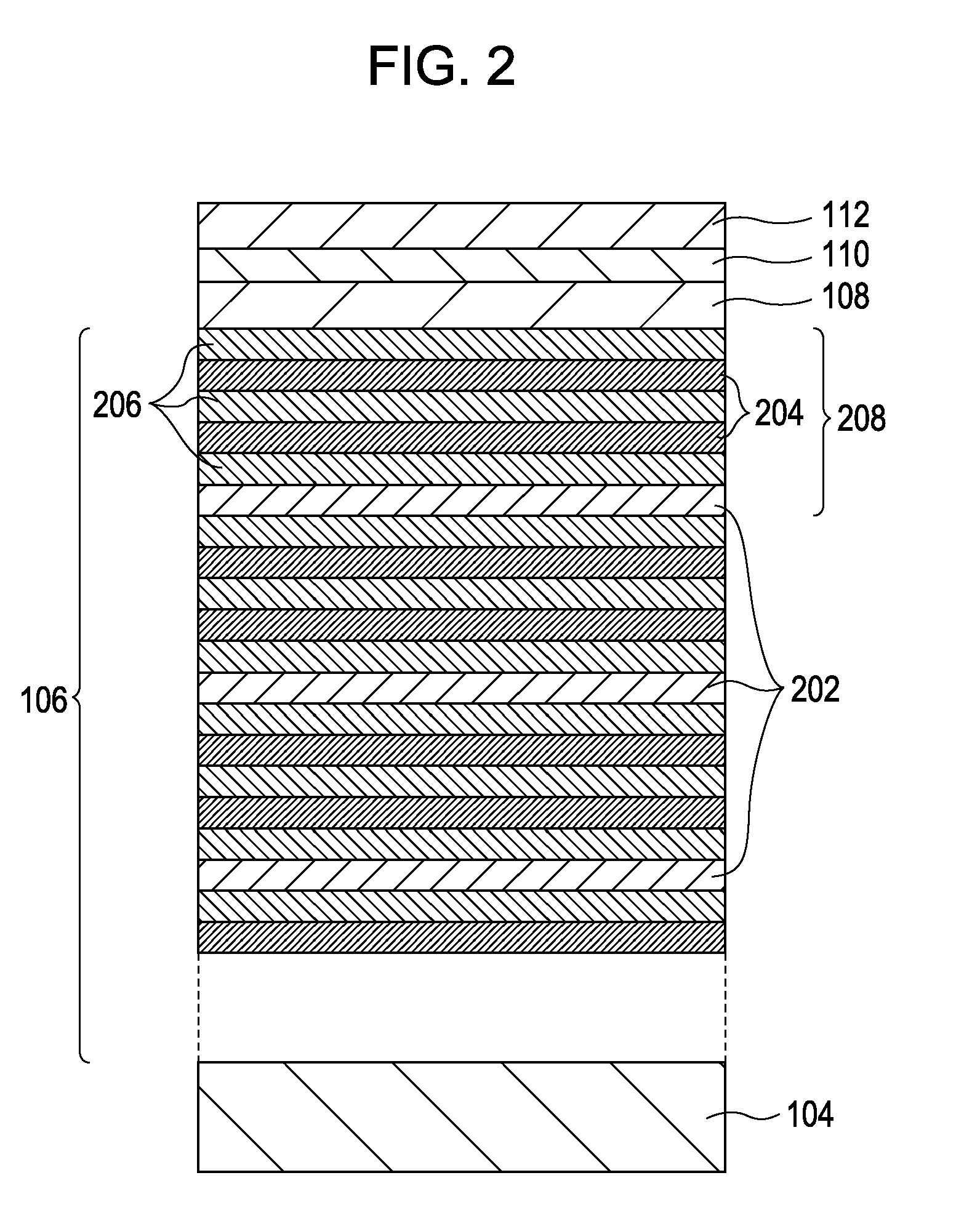
[0119]In Example 1, a configuration example of a vertical cavity surface emitting laser including one pair of multilayer mirrors, which lase at 680 nm and which are disposed opposing to each other, and an active layer disposed between these multilayer mirrors disposed opposing to each other will be described with reference to FIG. 1.

[0120]The surface emitting laser according to the present example is provided with an n-type multilayer mirror 106 including AlGaInP quaternary strain compensation layers 124 and p-type multilayer mirror 116 including the AlGaInP quaternary strain compensation layers 124. In this regard, as shown in FIG. 1, the AlGaInP quaternary strain compensation layers 124 are disposed uniformly on a strain compensation unit structure basis regardless of p-type multilayer mirror or n-type multilayer mirror.

[0121]The manner in which quaternary strain compensation layers are formed is shown in detail by a magnified diagram of the n-type multilayer mirror 106 shown in F...

example 2

[0148]In Example 2, a vertical cavity surface emitting laser including one pair of multilayer mirrors, which lase at 680 nm and which are disposed opposing to each other, and an active layer disposed between these multilayer mirrors disposed opposing to each other will be described with reference to FIG. 5.

[0149]In FIG. 5, the same configurations as those shown in FIG. 1 are indicated by the same reference numerals as those set forth above. Accordingly, further explanations thereof will not be provided, and only different structures will be explained.

[0150]In FIG. 5, reference numeral 502 denotes an n-type AlGaInP strain compensation layer. This layer in itself is the same as the n-type AlGaInP strain compensation layer 124 shown in FIG. 1, but arrangements in the p-type multilayer mirror and the n-type multilayer mirror are different from each other.

[0151]Here, in order to minimize the effect of heat on the GaInP strained quantum well active layer 110, a larger number of quaternary...

example 3

[0174]In Example 3, a vertical cavity surface emitting laser, which lases at 680 nm will be described with reference to FIG. 7. The vertical cavity surface emitting laser of the present example includes one pair of multilayer mirrors disposed opposing to each other and an active layer disposed between the multilayer mirrors.

[0175]In FIG. 7, the same configurations as those shown in FIG. 1 are indicated by the same reference numerals as those set forth above. Accordingly, further explanations thereof will not be provided, and only different structures will be explained. In FIG. 7, reference numeral 702 denotes an n-type AlGaInP strain compensation layer. The strain compensation layer 702 is of the same structure as the n-type AlGaInP strain compensation layer 124 shown in FIG. 1, but the arrangement in the multilayer mirror is different.

[0176]In the present example, in order to minimize the effect of heat on the GaInP strained quantum well active layer 110, a larger number of quatern...


PUM


Abstract

A surface emitting laser includes a pair of multilayer mirrors disposed opposing to each other, and an active layer disposed between the multilayer mirrors. In at least one multilayer mirror of the pair of multilayer mirrors, a plurality of first pair layers are stacked, each first pair layer is formed from a high-refractive index layer having a first strain and a low-refractive index layer having a second strain; and a second pair layer is included, the second pair layer is formed of one of the high-refractive index layer and the low-refractive index layer of the first pair layer in which one of the high-refractive index layer and the low-refractive index layer of the first pair layer is replaced with a layer formed from a quaternary or higher mixed crystal semiconductor material having a third strain.

Description

BACKGROUND OF THE INVENTION[0001]1. Field of the Invention[0002]The present invention relates to a surface emitting laser, a surface emitting laser array, and an optical apparatus including the surface emitting laser array.[0003]2. Description of the Related Art[0004]The surface emitting laser (SEL) is an important device for various optical applications, such as optical communications and electrophotographic printing. A well known type of surface emitting laser is the vertical cavity surface emitting laser (VCSEL). In a surface emitting laser, light can be taken in a direction perpendicular to a semiconductor substrate surface, which facilitates the formation of two-dimensional arrays by merely changing a mask pattern in element formation.[0005]Parallel processing through the use of a plurality of beams emitted from a thus formed two-dimensional array can achieve a high density and a high speed, so that various industrial applications are made possible.[0006]For example, the VCSEL ...

Claims


Application Information

Patent Timeline
Patent Type & Authority Applications(United States)
IPC IPC(8): H01S5/18H01S5/323
CPCB82Y20/00H01S5/18311H01S2301/173H01S5/34333H01S5/3201
Inventor TAKEUCHI, TETSUYA
Owner CANON KK
Why Eureka
Try Eureka