Laminated ceramic electronic component and method for manufacturing the same

a technology of electronic components and laminated ceramics, applied in the direction of ceramic layered products, chemistry apparatus and processes, layered products, etc., can solve the problems of difficult maintenance of multi-layer ceramic substrate reliability, requiring a lot of time for firing, and a complicated process, so as to improve the sinterability of the second ceramic layer, and reduce the softening point of the glass component

Inactive Publication Date: 2011-02-17
MURATA MFG CO LTD
View PDF1 Cites 7 Cited by
  • Summary
  • Abstract
  • Description
  • Claims
  • Application Information

AI Technical Summary

Benefits of technology

[0015]According to a preferred embodiment of the present invention, a method for manufacturing a laminated ceramic electronic component includes the steps of forming a green ceramic laminate and firing the green ceramic laminate, the green ceramic laminate including a first ceramic green layer which includes a first conductor pattern including Ag as a main component and which includes a first ceramic material including a first glass component, and a second ceramic green layer which includes a second conductor pattern including Ag as a main component, which includes a second ceramic material including a second glass component, and which has a composition in which Ag more easily diffuses than in the first ceramic green layer during firing. The first ceramic green layer is disposed along each of both main surfaces while at least a portion of the first conductor pattern is exposed on a surface.
[0016]According to another preferred embodiment of the present invention, the first glass component preferably has a higher softening point than the second glass component such that, in the second ceramic green layer, Ag more easily diffuses than in the first ceramic green layer during firing. For example, the first glass component preferably has a lower content of alkali metal oxide or a lower content of boron oxide than that of the second glass component, so that the first and second glass components have different softening points as described above.
[0020]According to another preferred embodiment of the present invention, the first ceramic green layer includes a composition in which Ag does not significantly diffuse during firing. Consequently, it is possible to improve migration resistance on a surface of the first ceramic layer produced by firing the first ceramic green layer.
[0021]On the other hand, the second ceramic green layer includes a composition in which Ag diffuses relatively easily during firing, and thus, the softening point of the glass component can be decreased by Ag diffusion. Consequently, it is possible to improve the sinterability of the second ceramic layer produced by firing the second ceramic green layer. Since the first ceramic layer is disposed only in a surface layer portion of the laminated ceramic electronic component, as described above, the improvement in sinterability of the second ceramic layer can improve the reliability and strength of the entire the laminated ceramic electronic component. In addition, moisture does not significantly enter the inner layer portion at which the second ceramic layer is disposed, thereby not significantly influencing the migration resistance.
[0022]According to various preferred embodiments of the present invention, the laminated ceramic electronic component is capable of achieving high reliability and strength while maintaining migration resistance. In addition, firing can be performed in an oxidizing atmosphere in the firing step for producing the laminated ceramic electronic component.
[0023]According to a preferred embodiment of the present invention, the first ceramic material and the second ceramic material include common constituent elements, and thus, an intermediate product is not formed between the first ceramic green layer and the second ceramic green layer. As a result, the bonding strength between the first ceramic layer and the second ceramic layer after firing is improved.

Problems solved by technology

As a result, it may be difficult to maintain the reliability of the multilayer ceramic substrate.
According to Japanese Examined Patent Application Publication No 3-78798, a conductor pattern made of a Cu-based conductor is provided, and thus, firing cannot be performed in an oxidizing atmosphere.
However, this method has a problem of requiring a lot of time for firing and a complicated process.
However, in this case, the firing atmosphere is limited, which causes difficulties in adjusting the atmosphere.

Method used


Image

  • Laminated ceramic electronic component and method for manufacturing the same
  • Laminated ceramic electronic component and method for manufacturing the same
  • Laminated ceramic electronic component and method for manufacturing the same

Examples


Embodiment Construction

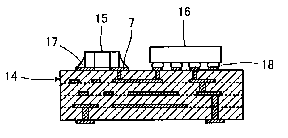
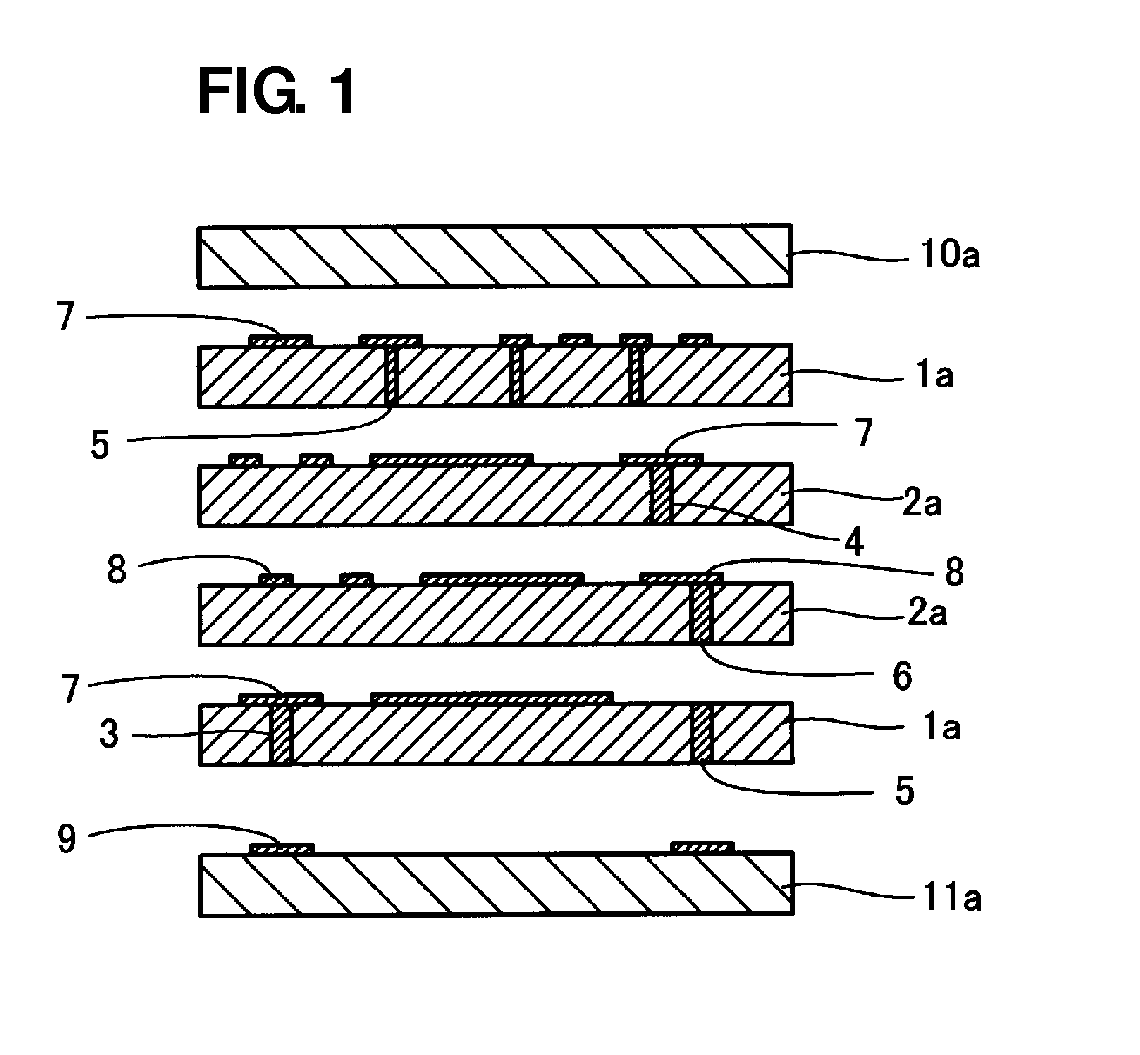
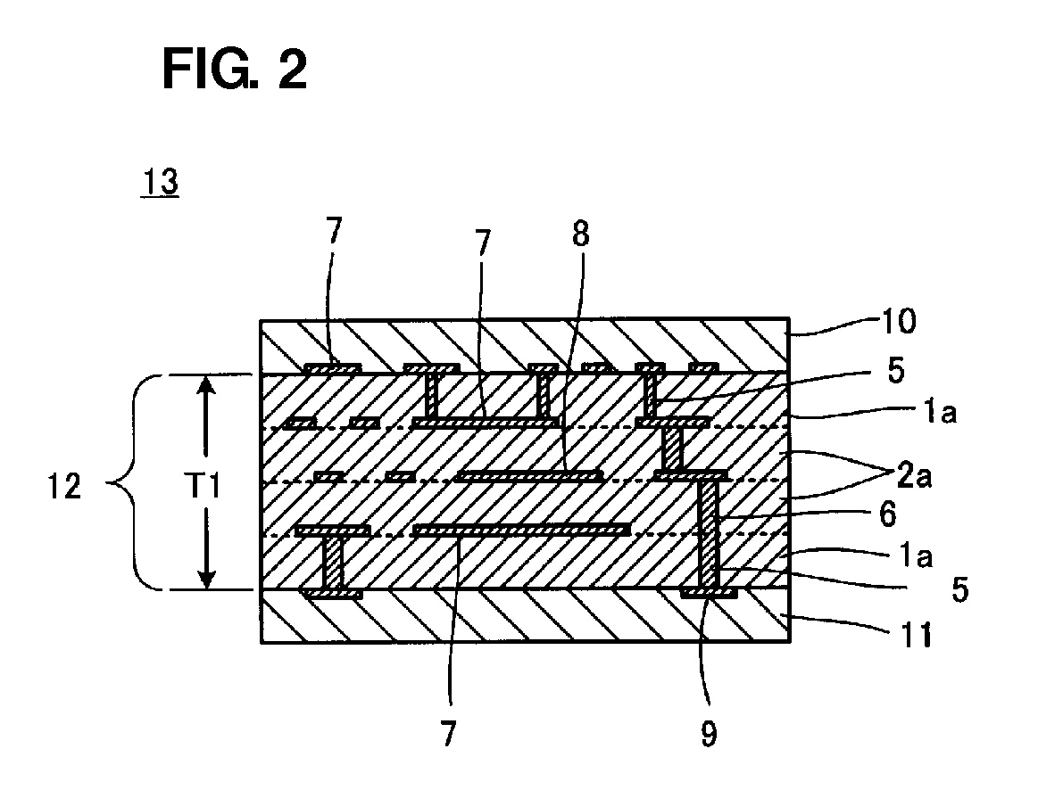
[0030]FIGS. 1 to 4 are sectional views for explaining a method for manufacturing a laminated ceramic electronic component according to a preferred embodiment of the present invention. In particular, these figures show a method for manufacturing a multilayer ceramic substrate.

[0031]As shown in FIG. 1, first ceramic green sheets 1a defining first ceramic layers 1 (refer to FIG. 4) are prepared, and second ceramic green sheets 2a defining second ceramic layers 2 (refer to FIG. 4) are prepared. The first ceramic green sheets 1a and the second ceramic green sheets 2a include first and second low-temperature sinterable materials including first and second glass components, respectively.

[0032]The ceramic green sheets 1a and 2a are each produced by dispersing a ceramic material powder in a vehicle including a binder, a solvent, a plasticizer, and other suitable constituents to prepare a slurry, and forming the resultant slurry into a sheet shape by a casting method, such as a doctor blade m...


PUM

PropertyMeasurementUnit
distanceaaaaaaaaaa
average particle diameteraaaaaaaaaa
temperaturesaaaaaaaaaa

Abstract

In a method for manufacturing a laminated ceramic electronic component, in order to form a green ceramic laminate to be fired, first ceramic green layers which include first conductor patterns including Ag as a main component and which include a first ceramic material including a first glass component are disposed in surface layer portions. Second ceramic green layers which include second conductor patterns including Ag as a main component, which include a second ceramic material containing a second glass component, and which include a composition in which Ag diffuses than more easily in the first ceramic green layer during firing are disposed in inner layer portions. The green ceramic laminate is fired to produce a multilayer ceramic substrate.

Description

BACKGROUND OF THE INVENTION[0001]1. Field of the Invention[0002]The present invention relates to a laminated ceramic electronic component and a method for manufacturing the same. In particular, the present invention relates to an improvement for suppressing Ag migration on a surface of a laminated ceramic electronic component.[0003]2. Description of the Related Art[0004]An example of a multilayer ceramic substrate includes a plurality of laminated ceramic layers and conductor patterns provided on surfaces and inside the substrate. Examples of the conductor patterns include an in-plane conductor extending in a planar direction of a ceramic layer and an interlayer connecting conductor (typically a via hole conductor) extending to pass through a ceramic layer in the thickness direction.[0005]In general, surface-mount type electronic components, such as a semiconductor device or a chip laminated capacitor, for example, are mounted and wired together on such a multilayer ceramic substrat...

Claims


Application Information

Patent Timeline
Patent Type & Authority Applications(United States)
IPC IPC(8): H05K1/09B29C65/02
CPCB32B18/00C04B2237/343C04B2237/562H05K3/4629H05K3/4688H01L2924/19105C04B2237/62C04B2237/68C04B2237/702H01L2224/16225H01L2924/15192H05K2203/308
Inventor CHIKAGAWA, OSAMUIKEDA, TETSUYA
Owner MURATA MFG CO LTD
Why Eureka
Try Eureka