Method for manufacturing microcrystalline semiconductor film and thin film transistor

a technology of microcrystalline semiconductors and thin film transistors, applied in the direction of coatings, chemical vapor deposition coatings, electric discharge tubes, etc., can solve the problems of poor electric characteristics of thin film transistors and low film density, and achieve small off-current, large on-current, and high crystallinity

Inactive Publication Date: 2011-02-17
SEMICON ENERGY LAB CO LTD
View PDF40 Cites 31 Cited by
  • Summary
  • Abstract
  • Description
  • Claims
  • Application Information

AI Technical Summary

Benefits of technology

[0013]As described above, a microcrystalline semiconductor film with high crystallinity can be manufactured. Further, a thin film transistor with small off-current and large on-current can be manufactured with high productivity.

Problems solved by technology

An inversely-staggered thin film transistor in which a microcrystalline semiconductor film is used for a channel formation region has problems in that crystallinity of the microcrystalline semiconductor film in an interface region between a gate insulating film and the microcrystalline semiconductor film is low and electric characteristics of the thin film transistor are poor.

Method used


Image

  • Method for manufacturing microcrystalline semiconductor film and thin film transistor
  • Method for manufacturing microcrystalline semiconductor film and thin film transistor
  • Method for manufacturing microcrystalline semiconductor film and thin film transistor

Examples


embodiment 1

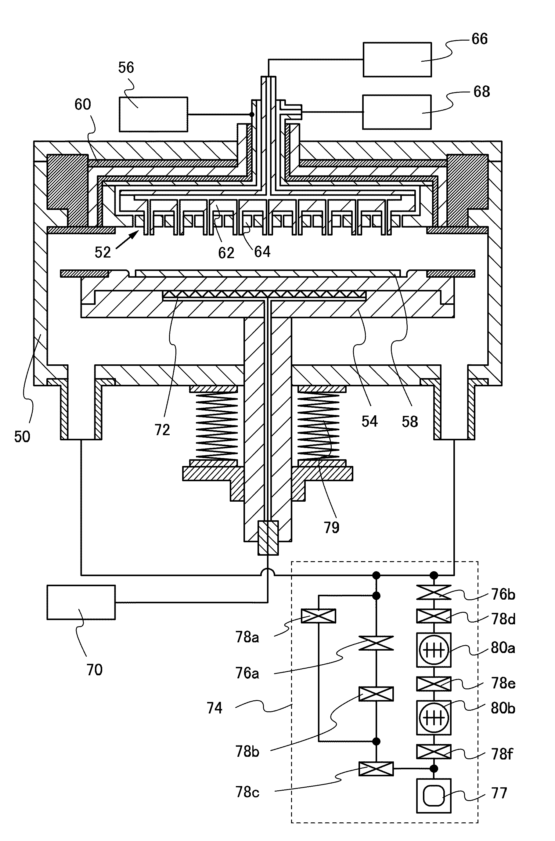
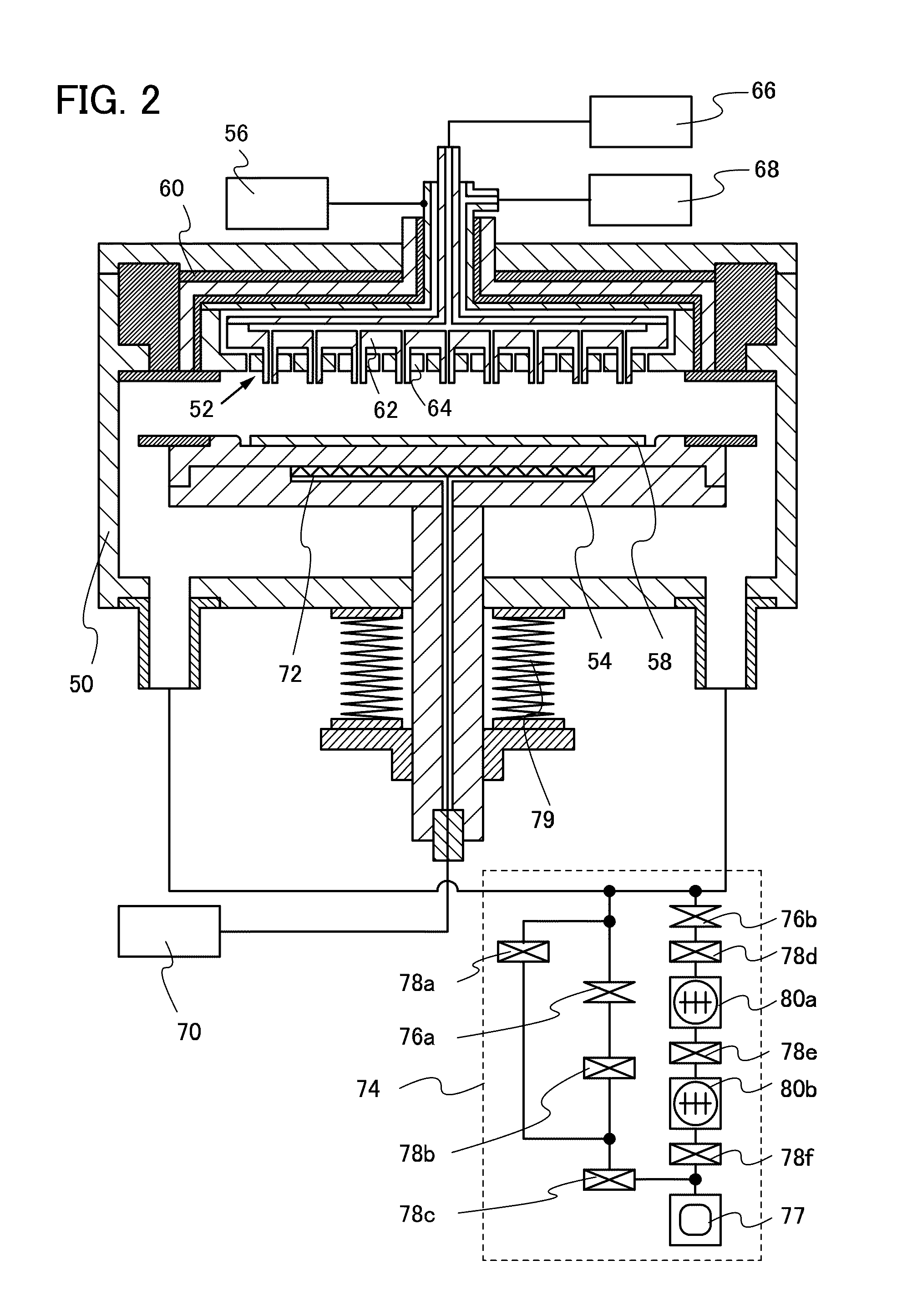
[0031]In this embodiment, a method for forming a microcrystalline semiconductor film with high crystallinity is described with reference to FIGS. 1A and 1B, FIG. 2, FIG. 3, FIG. 4 and FIG. 5.

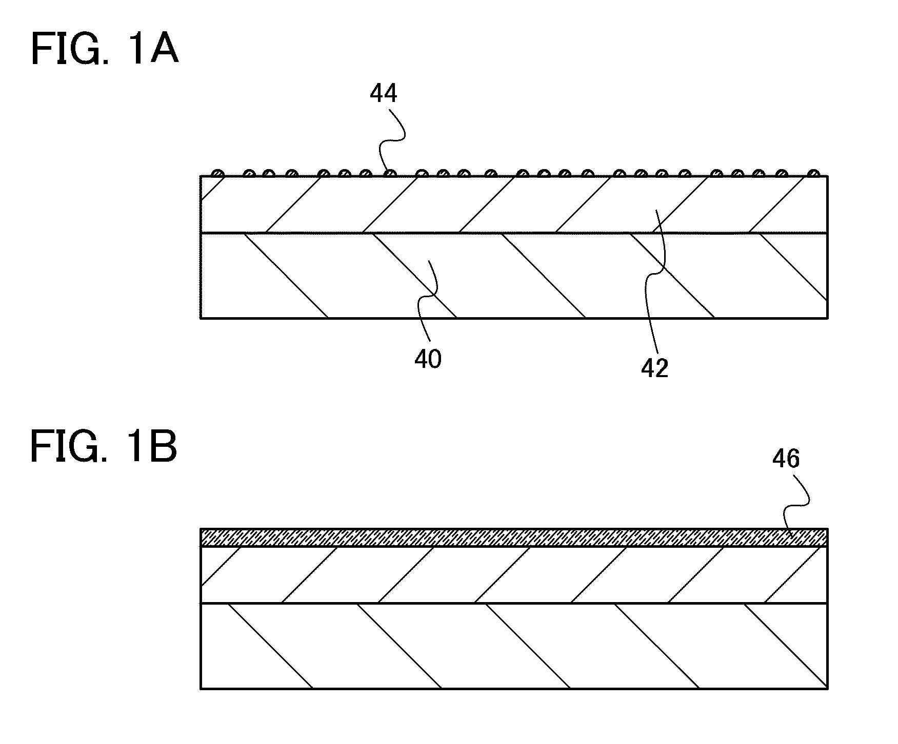
[0032]In a method for forming a microcrystalline semiconductor film shown in this embodiment, crystal particles 44 (also referred to as nanoparticles) are formed over a base film 42 formed over a substrate 40 as shown in FIG. 1A. Next, by depositing a microcrystalline semiconductor film over the base film 42 and the crystal particles 44, crystals are grown using the crystal particles 44 as crystal nuclei, whereby a microcrystalline semiconductor film 46 can be formed, as shown in FIG. 1B.

[0033]The crystal particle 44 is crystalline silicon, crystalline germanium, crystalline silicon germanium, or the like having a crystal grain size of several nanometers. The crystal particle 44 includes therein a crystallite which is a minute crystal regarded as a single crystal. Further, the crystal particle 4...

embodiment 2

[0069]In this embodiment, a structure of a thin film transistor including a microcrystalline semiconductor film formed by the method described in Embodiment 1 is described with reference to FIGS. 6A to 6C.

[0070]The microcrystalline semiconductor film formed by the method described in Embodiment 1 can be used for a channel formation region of the thin film transistor. As the thin film transistor, both a bottom-gate thin film transistor and a top-gate thin film transistor can be used; however, characteristics of the thin film transistor can be improved by using a bottom-gate thin transistor in particular. Here, a typical structure of a bottom-gate thin film transistor is explained with reference to FIGS. 6A to 6C.

[0071]A thin film transistor shown in FIG. 6A is a channel-etched thin film transistor. A gate electrode 103 is formed over a substrate 101, and a gate insulating film 104 is formed to cover the substrate 101 and the gate electrode 103. A microcrystalline semiconductor film 1...

embodiment 3

[0096]In this embodiment, a method for manufacturing the thin film transistor shown in FIG. 6C, which is one embodiment of the thin film transistors described in Embodiment 2, will be described with reference to FIGS. 7A to 7D, FIGS. 8A to 8C, FIGS. 9A and 9B, FIG. 10, and FIGS. 11A and 11B.

[0097]Here, all thin film transistors formed over one substrate preferably have the same conductivity type because the number of manufacturing steps can be reduced. In view of the above, a method for manufacturing an n-channel thin film transistor will be described in this embodiment.

[0098]As shown in FIG. 7A, a gate electrode 303 is formed over a substrate 301. Then, after a gate insulating film 304 is formed so as to cover the gate electrode 303, crystal particles 305 are formed over the gate insulating film 304 by the method for forming crystal particles described in Embodiment 1.

[0099]As the substrate 301, the substrate 101 described in Embodiment 2 can be used as appropriate.

[0100]The materi...


PUM

PropertyMeasurementUnit
frequencyaaaaaaaaaa
frequencyaaaaaaaaaa
frequencyaaaaaaaaaa

Abstract

A microcrystalline semiconductor film with high crystallinity is manufactured. In addition, a thin film transistor with excellent electric characteristics and high reliability, and a display device including the thin film transistor are manufactured with high productivity. A deposition gas containing silicon or germanium is introduced from an electrode including a plurality of projecting portions provided in a treatment chamber of a plasma CVD apparatus, glow discharge is caused by supplying high-frequency power, and thereby crystal particles are formed over a substrate, and a microcrystalline semiconductor film is formed over the crystal particles by a plasma CVD method.

Description

BACKGROUND OF THE INVENTION[0001]1. Field of the Invention[0002]The present invention relates to a microcrystalline semiconductor film and a thin film transistor, a manufacturing method thereof, and a display device to which the thin film transistor is applied.[0003]2. Description of the Related Art[0004]As one type of field-effect transistor, a thin film transistor whose channel formation region is formed using a semiconductor film that is formed over a substrate having an insulating surface is known. Techniques in which microcrystalline silicon is used for the semiconductor film in the thin film transistor have been disclosed (see Patent Documents 1 to 3). A typical application of the thin film transistor is a liquid crystal television device, in which the thin film transistor has been put to practical use as a switching transistor for each pixel that constitutes a display screen.REFERENCEPatent Document[Patent Document 1] Japanese Published Patent Application No. 2009-044134[Pate...

Claims


Application Information

Patent Timeline
Patent Type & Authority Applications(United States)
IPC IPC(8): H01L21/20
CPCC23C16/24C23C16/4404C23C16/45565C23C16/45574C23C16/5096H01J37/3244H01L29/78696H01J37/32541H01L21/02532H01L21/02595H01L21/0262H01L29/04H01L29/66765H01J37/32449
Inventor YAMAZAKI, SHUNPEISUZUKI, YUKIEARAI, YASUYUKIINOUE, TAKAYUKIKIKUCHI, ERUMU
Owner SEMICON ENERGY LAB CO LTD
Why Eureka
Try Eureka