

Photovoltaic Cell on Substrate
- Summary
- Abstract
- Description
- Claims
- Application Information
AI Technical Summary
Benefits of technology
Problems solved by technology
Method used
Image

Examples
Embodiment Construction
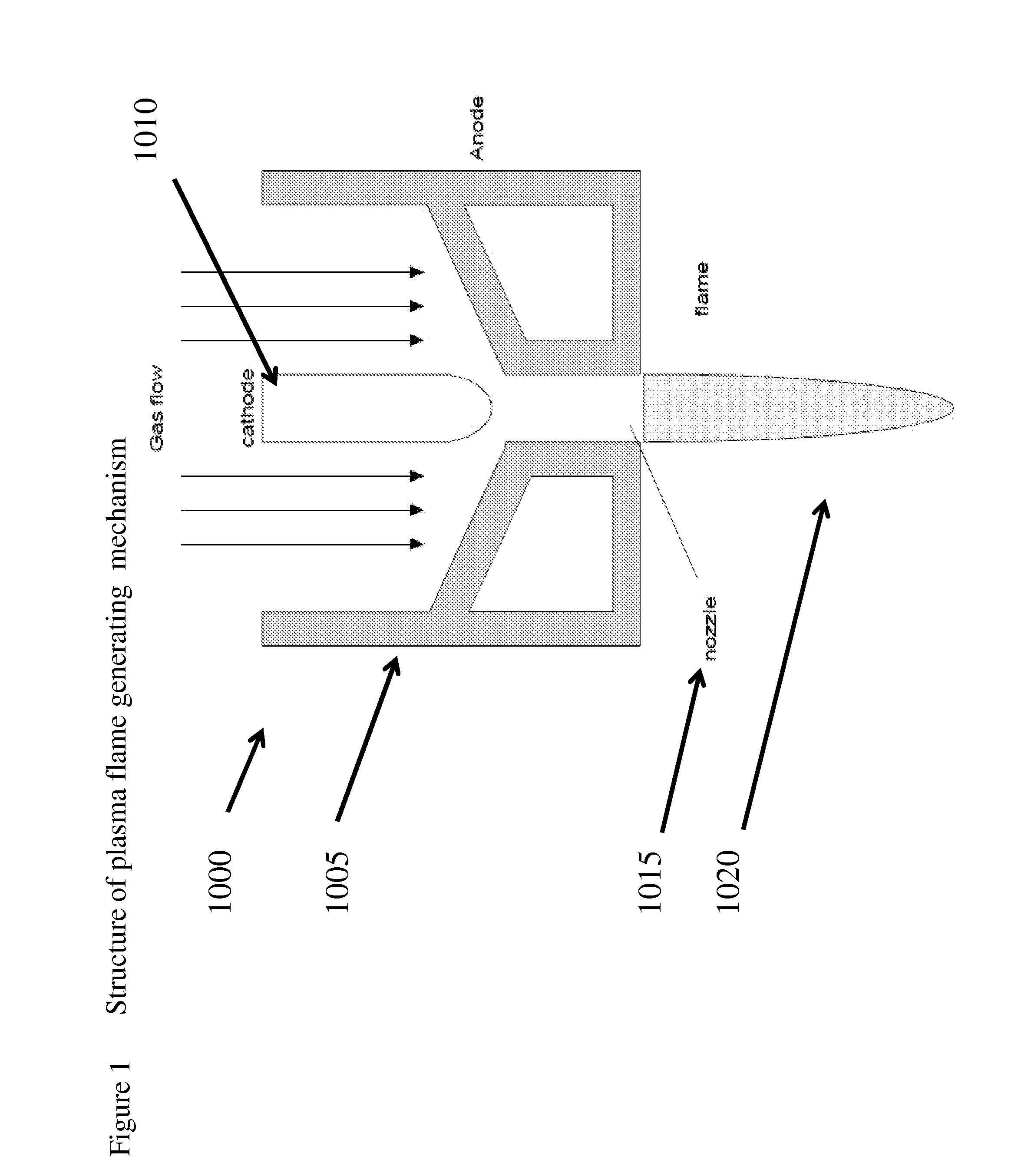
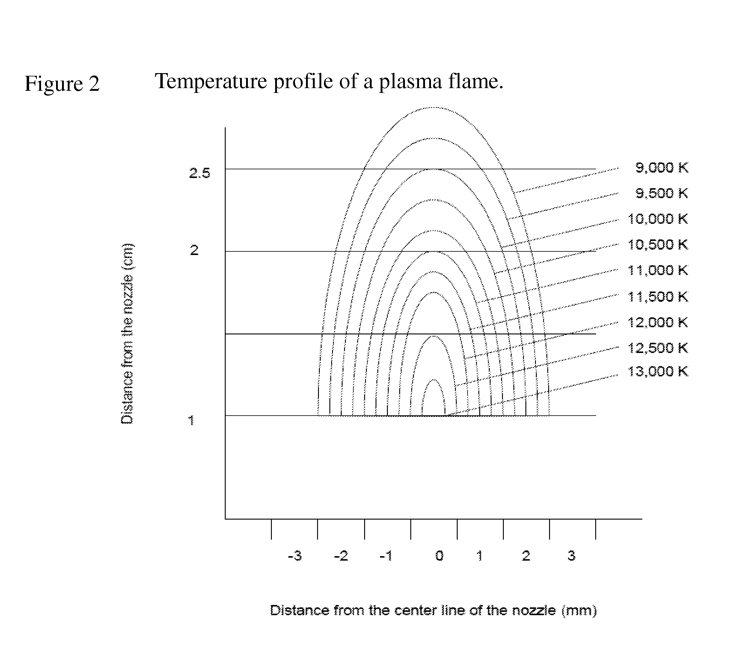
[0027]One embodiment comprises deposition by high-purity plasma spray of one or more layers of silicon and / or dielectric. The generation of high temperature plasma is typically done with argon, although other gases can be used. Passing a high current, on the order of 500 amperes, through the argon gas, between the cathode 1010 and anode 1005 generates a plasma 1020. This current heats the argon and strips the argon of its electrons. The flow of the plasma exiting nozzle 1015 is determined by the flow of the gas feed into the plasma generator (plasma gun or plasma torch1000); note FIG. 1. Typical flow rates for commercial plasma guns such as Sulzer Metco 9B gun are on the order of 100+ SCFH at an input pressure of 75 psig. Frequently it is advantageous to mix a secondary gas in with the primary plasma gas to promote higher temperatures. Typical secondary gasses to work with argon are hydrogen and helium. Typically the mix of the secondary gas will be at around 10% of the primary gas ...
PUM
 Abstract
Description
Claims
Application Information