Optical semiconductor device and method for manufacturing the same
a technology of optical semiconductors and semiconductor devices, which is applied in the direction of semiconductor devices, diodes, electrical devices, etc., can solve the problems of serious damage to light having a short wavelength in the vicinity of the silicon surface, and achieve the effects of high light receiving sensitivity, high speed and high speed
- Summary
- Abstract
- Description
- Claims
- Application Information
AI Technical Summary
Benefits of technology
Problems solved by technology
Method used
Image

Examples
embodiment 1
Preferred Embodiment 1 of Method for Manufacturing Optical Semiconductor Device
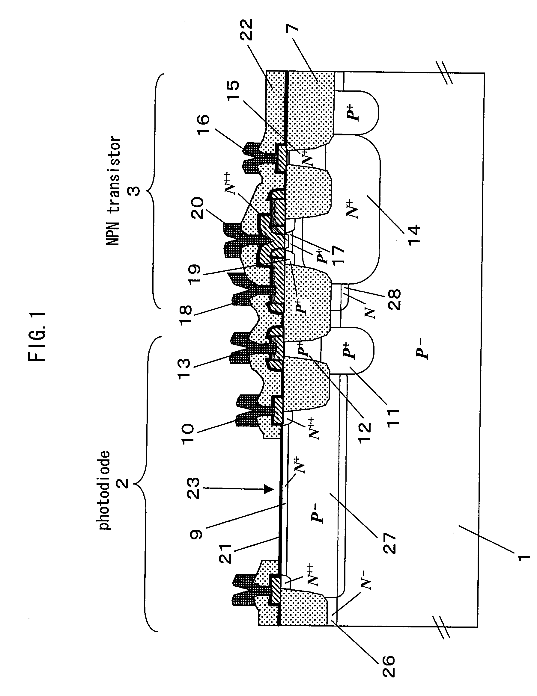
[0150]FIGS. 7A-7E are sectional views illustrating processing steps of a preferred embodiment 1 of a method for manufacturing the optical semiconductor device according to the present invention. 40 denotes a photodiode, 41 denotes an NPN transistor, 42 denotes a low concentration p-type silicon substrate, 43 denotes a p-type embedding layer, 44 denotes an n-type embedding layer of a collector of the NPN transistor 41, 45 denotes a low concentration n-type epitaxial layer (second epitaxial layer), 46 denotes a low concentration p-type anode diffusion layer (first diffusion layer), 47 denotes an n-type well layer having a concentration higher than that of the n-type epitaxial layer 45, 48 denotes a LOCOS isolation layer, and 49 denotes a high concentration n-type cathode layer (second diffusion layer).
[0151]First, the p-type embedding layer 43 and the n-type embedding layer 44 are selectively formed in the ...
embodiment 2
Preferred Embodiment 2 of Method for Manufacturing Optical Semiconductor Device
[0162]FIGS. 8A-8E are sectional views illustrating processing steps of a preferred embodiment 2 of the method for manufacturing the optical semiconductor device according to the present invention. In the drawings, 50 denotes a low concentration p-type anode embedding layer (second embedding layer). The rest of the constitution is the same as illustrated in FIG. 7.
[0163]First, the p-type embedding layer 43, n-type embedding layer 44 and anode embedding layer (second embedding layer) 50 are selectively formed in the silicon substrate 42 by means of the ion implantation or the like (see FIG. 8A). In the formation, conditions are set so that the anode embedding layer (second embedding layer) 50 has its dopant concentration peak in the vicinity of the surface of the silicon substrate 42 (for example, acceleration energy: 30 keV, dosing amount: 1×1011 cm−2).
[0164]Next, the n-type epitaxial layer (second epitaxi...
embodiment 3
Preferred Embodiment 3 of Method for Manufacturing Optical Semiconductor Device
[0174]FIGS. 9A-9E are sectional views illustrating processing steps of a preferred embodiment 3 of the method for manufacturing the optical semiconductor device according to the present invention. In the drawings, 51 denotes a low concentration p-type anode diffusion layer (third diffusion layer). The rest of the constitution is the same as illustrated in FIG. 8.
[0175]First, the p-type embedding layer 43, n-type embedding layer 44 and anode embedding layer (second embedding layer) 50 are selectively formed in the silicon substrate 42 by means of the ion implantation or the like (FIG. 9A). In the formation, conditions are set so that the anode embedding layer (second embedding layer) 50 has its dopant concentration peak in the vicinity of the surface of the silicon substrate 42 (for example, acceleration energy: 30 keV, dosing amount: 1×1011 cm−2).
[0176]Next, the n-type epitaxial layer (second epitaxial la...
PUM
 Abstract
Description
Claims
Application Information
 - Generate Ideas
- Intellectual Property
- Life Sciences
- Materials
- Tech Scout
- Unparalleled Data Quality
- Higher Quality Content
- 60% Fewer Hallucinations
Browse by: Latest US Patents, China's latest patents, Technical Efficacy Thesaurus, Application Domain, Technology Topic, Popular Technical Reports.
© 2025 PatSnap. All rights reserved.Legal|Privacy policy|Modern Slavery Act Transparency Statement|Sitemap|About US| Contact US: help@patsnap.com