

Semiconductor phosphor nanoparticle including semiconductor crystal particle made of 13th family-15th family semiconductor
a technology of semiconductor crystal particles and semiconductors, applied in the field of semiconductor crystal particles of 13th family-15th family semiconductors, can solve the problems of difficult to stably disperse phosphor, difficult to separate and purify only phosphor from raw materials, aggregation of phosphor at room temperature, etc., to suppress the inactivation of excitation energy, high luminous efficiency, and stable cap a surface defect of semiconductor crystals
- Summary
- Abstract
- Description
- Claims
- Application Information
AI Technical Summary
Benefits of technology
Problems solved by technology
Method used
Image

Examples
first embodiment
[0022]The present invention will be described in more detail below. While the description is made with reference to the accompanying drawings in the following description of embodiments, constituents represented by the identical reference symbol denote the identical portions or corresponding portions in the drawings of the present specification. Since relationship between dimensions such as length, size and width in the drawings is appropriately varied for clarity and simplification, the dimensions are not actual dimensions.
[0023]
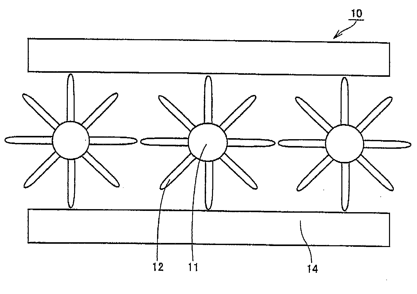
[0024]FIG. 1 is a sectional view schematically showing one preferred example of a basic structure of a semiconductor phosphor nanoparticle according to the present embodiment. As shown in FIG. 1, a semiconductor phosphor nanoparticle 10 of the present embodiment includes a semiconductor crystalline particle 11, a modified organic compound 12 coating semiconductor crystalline particle 11, and a layered compound 14 sandwiching modified organic compound 12 bet...
second embodiment
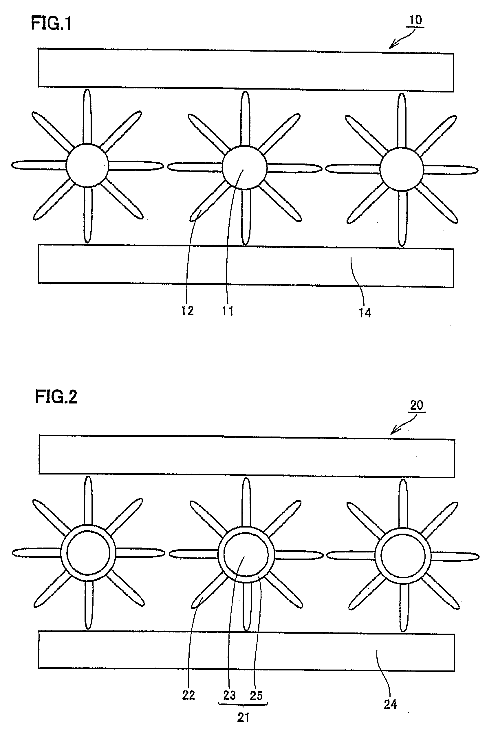
[0060]The semiconductor phosphor nanoparticle of the present embodiment is characterized by using a semiconductor crystalline particle having a core / shell structure. FIG. 2 is a view schematically showing a basic structure of a semiconductor phosphor nanoparticle where a semiconductor crystalline particle has a core / shell structure.
[0061]In a semiconductor phosphor nanoparticle 20 of the present embodiment, as shown in FIG. 2, a semiconductor crystalline particle 21 includes a semiconductor crystal core 23, and a shell layer 25 coating semiconductor crystal core 23.
[0062]Semiconductor phosphor nanoparticle 20 of the present embodiment includes a modified organic compound 22 binding to a surface of shell layer 25, and a layered compound 24 containing semiconductor crystalline particle 21 protected with modified organic compound 22. Semiconductor phosphor nanoparticle 20 of the present embodiment will be described below.
[0063]
[0064]When semiconductor crystalline particle 21 has a core...
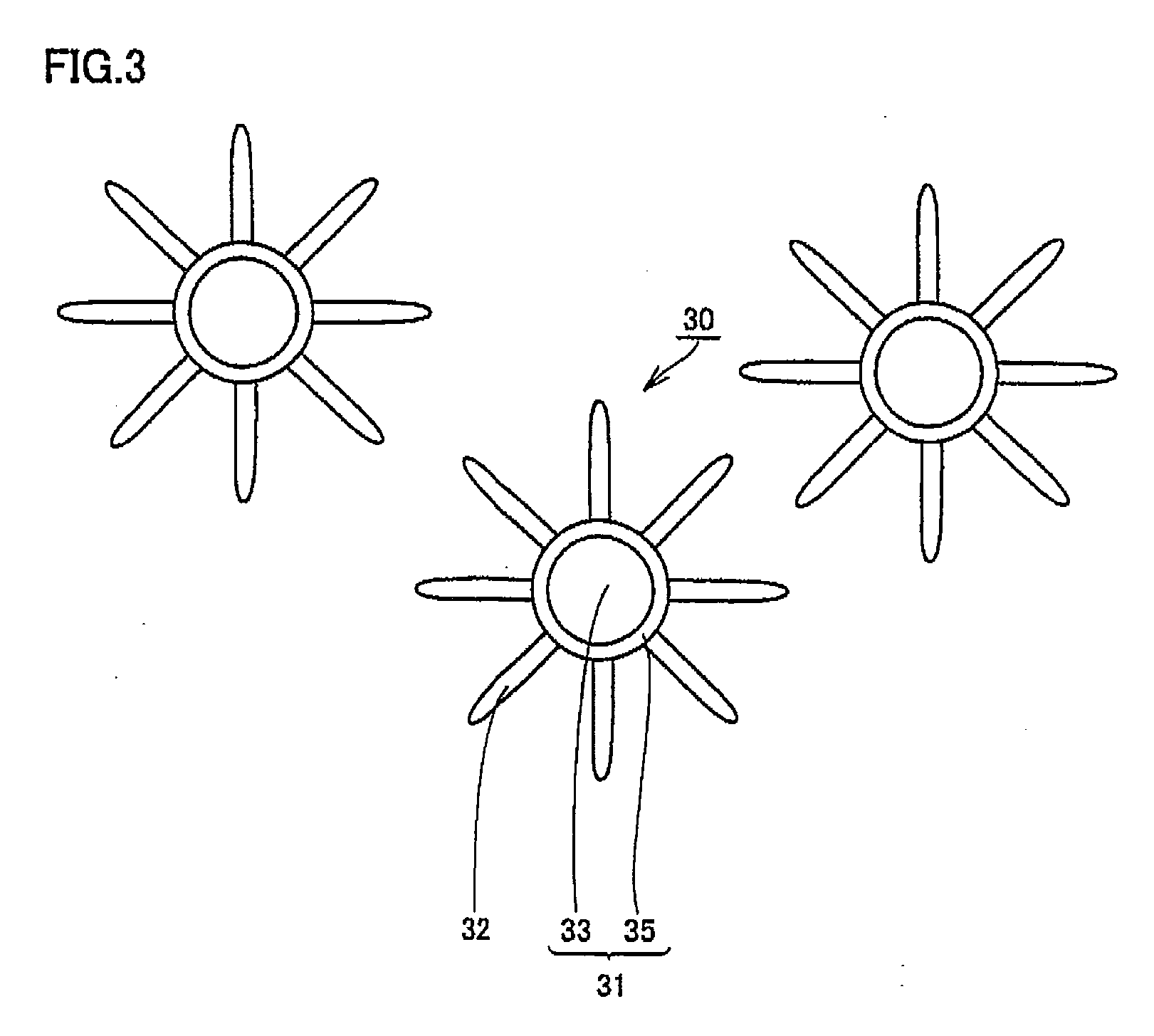
example 1
[0072]In the present Example, a semiconductor phosphor nanoparticle capable of absorbing excitation light to emit red light was prepared by a hot soap method. As shown in FIG. 2, semiconductor phosphor nanoparticle 20 includes semiconductor crystal core 23 made of InN, shell layer 25 made of GaN, modified organic compound 22 made of hexadecylamine (HDA) and layered compound 24 made of vanadium oxide. A method for producing the same will be described specifically below.
[0073]First, semiconductor crystal core 23 made of an InN crystal was synthesized by a thermal decomposition reaction of 1 mmol of tris(dimethylamino)indium and 2 mmol of HDA in 30 ml of a 1-octadecene solution. By adjusting a mean particle diameter of semiconductor crystal core 23 to 5 nm, a luminous wavelength was adjusted to 620 nm so as to exhibit red luminescence.
[0074]As a result of the measurement of semiconductor crystal core 23 by X-ray diffraction, a mean particle diameter of a semiconductor crystal core esti...
PUM
 Abstract
Description
Claims
Application Information