Novel process method for post plasma etch treatment

Inactive Publication Date: 2011-03-31
HEADWAY TECH INC
View PDF10 Cites 7 Cited by
  • Summary
  • Abstract
  • Description
  • Claims
  • Application Information

AI Technical Summary

Benefits of technology

[0013]It is another objective of the invention to use a high-enough temperature to eliminate or burn away the residual

Problems solved by technology

The heavy polymer deposition resulting from the DRIE process cannot stick to the sidewall permanently and will adversely affect the performance of the device.
While a regular wet-cleaning process can effectively remove the deposited polymer and other etching residuals for low aspect ratio or shallow structures (trenches, holes, circulars and so on), it is difficult to clean the high aspect ratio (HAR) structures with small etching feature sizes such as a few to tens micrometers.
For high DWAR and LWAR structures, the solution of the wet-cleaning chemicals may not easily flow in and out of the structures because of the liquid stiction and capillary effect.
Thus, polymer pieces will stay inside or around the structures and cause problems later.
The situation could become worse during the drying process after using water to rinse the cleaning chemicals from the wafer.
The heat applied to vaporize the trapped water will cause water

Method used


Image

  • Novel process method for post plasma etch treatment
  • Novel process method for post plasma etch treatment
  • Novel process method for post plasma etch treatment

Examples


Embodiment Construction

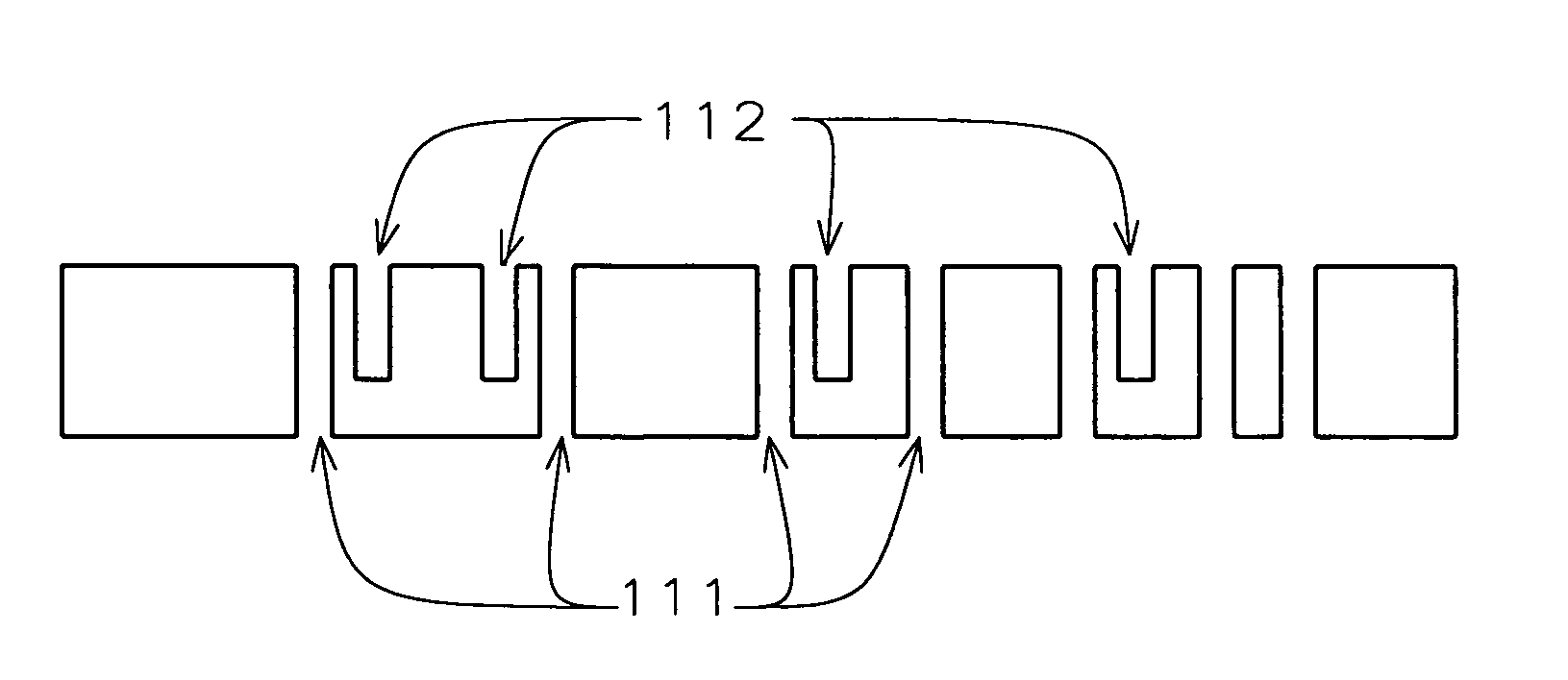
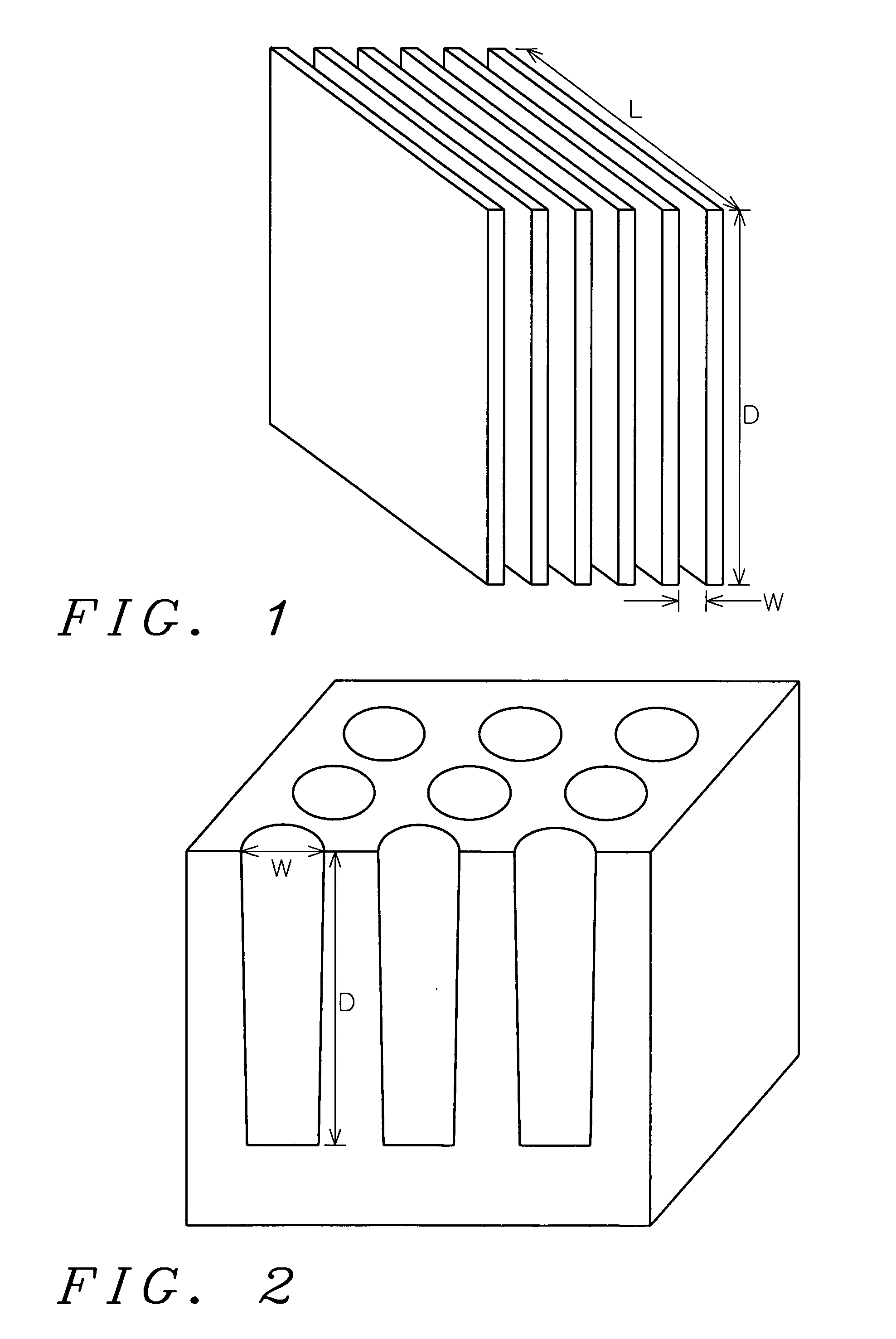
[0028]The present invention proposes three novel post-etch treatment methods that can be used to remove the residual polymers after DRIE etching. The methods are called post-etch dry-cleaning processes as opposed to the wet-cleaning processes usually used after plasma etching. In the dry-cleaning processes of the invention, after plasma etching, the wafers are placed in an environment such as a hot oven, a laser beam or a fire flame where the temperature is high enough that the polymers will be burned and decomposed into small molecules, then evaporated and pumped away. If not, then the polymers may be shrunken into very small pieces which either fall out by themselves or are blown out of the structure, or their sizes become so small and stick to sidewalls permanently that they would not interfere with the performance of the devices.

[0029]The traditional post-etch treatment method to clean the residues after plasma etching is so-called wet-cleaning in which the etched wafers are imm...


PUM


Abstract

A method of fabricating a wafer comprising MEMS devices comprises etching trenches or vias into the wafer using a deep reactive ion etching process wherein this process forms residual polymers on sidewalls of the trenches or vias. The wafer is exposed to a dry-cleaning process wherein residual polymers are removed. The dry-cleaning process comprises hot oven baking, combustion, or laser beam illumination.

Description

BACKGROUND OF THE INVENTION[0001](1) Field of the Invention[0002]This invention is related to MEMS devices, and more particularly, to methods of removing residual polymers in the fabrication of MEMS devices.[0003](2) Description of the Related Art[0004]Micro-electro-mechanical systems (MEMS), the smallest functional machines that can be manufactured currently, are made up of components ranging from a few micrometers to several millimeters in size. MEMS, a rapidly growing semiconductor field, have many important practical and potential commercial applications. There are a range of commercially available MEMS products including gyroscopes, pressure sensors, fluid regulators, optical switches, displays, mass data storage, biological sensors and chemical controllers.[0005]MEMS can be fabricated using semiconductor integrated circuit technologies. The basic procedures capable of manufacturing silicon based MEMS devices are: ingot growth and slicing, film preparation or deposition, wafer ...

Claims


Application Information

Patent Timeline
IPC IPC(8): H01L21/3065
CPCB81C1/00857B81C2201/0132H01L21/67109H01L21/67028H01L21/67103H01L21/02057
Inventor MAO, GUOMIN
Owner HEADWAY TECH INC
Why Eureka
Try Eureka