

Optoelectronic devices with laminate leadless carrier packaging in side-looker or top-looker device orientation
a leadless carrier and optoelectronic technology, applied in the direction of solid-state devices, basic electric elements, electric devices, etc., can solve the problems of heterogeneous semiconductors, low throughput assembly lines, and small wafer sizes, and achieve high stress
- Summary
- Abstract
- Description
- Claims
- Application Information
AI Technical Summary
Benefits of technology
Problems solved by technology
Method used
Image

Examples
Embodiment Construction
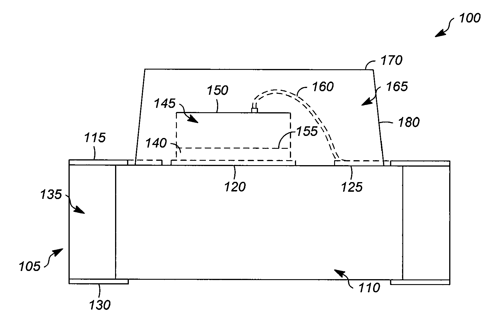
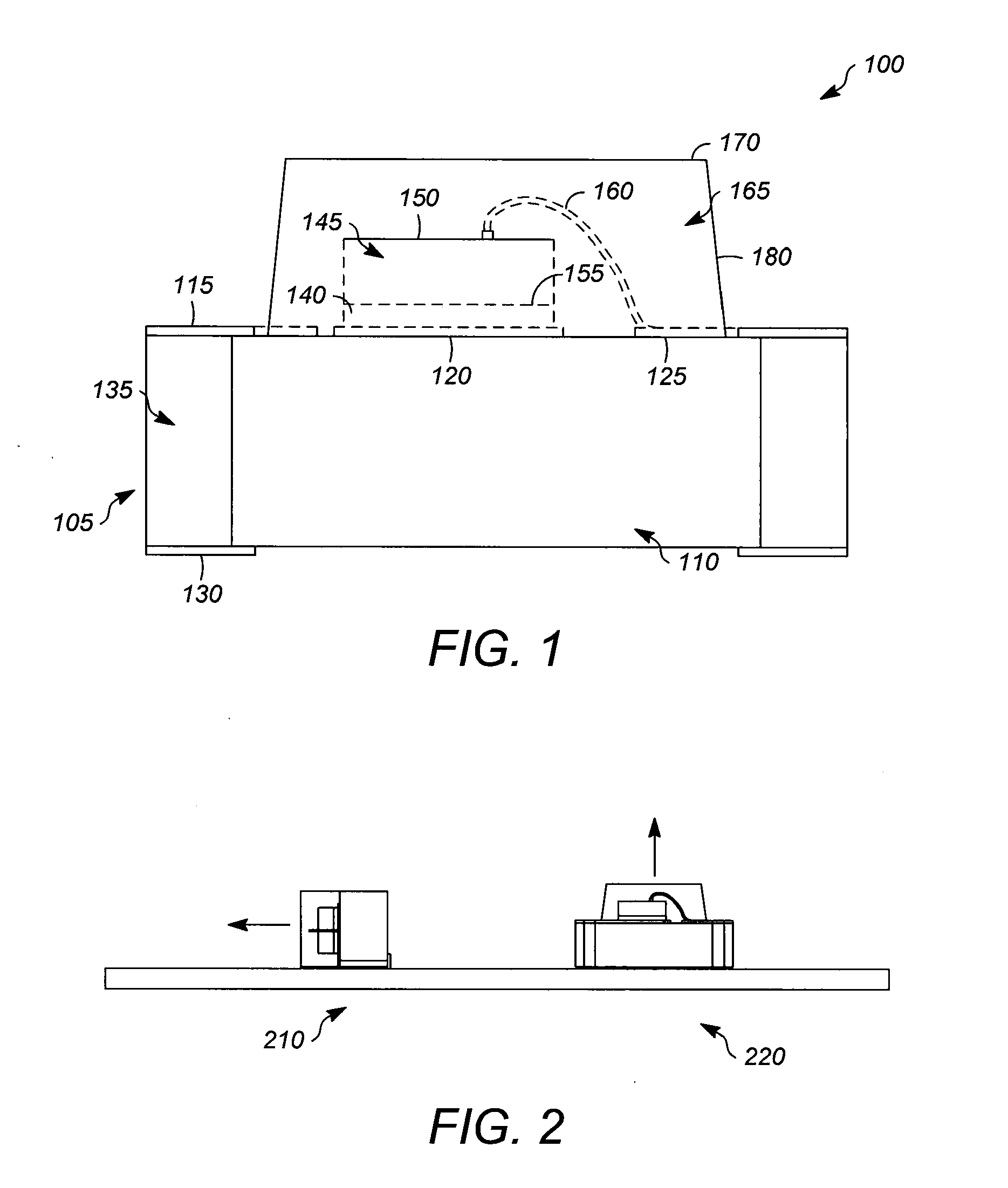
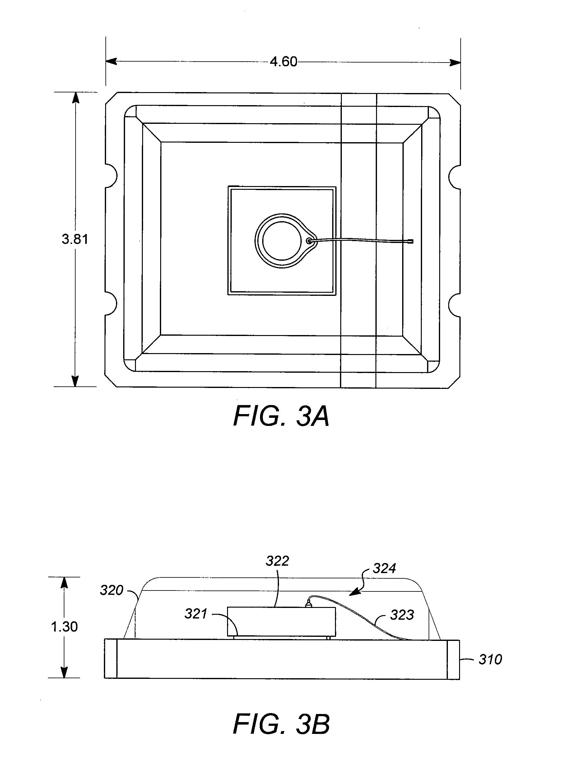
[0029]The following description is presented to enable a person of ordinary skill in the art to make and use the invention, and is provided in the context of particular applications and their requirements. Various modifications to the embodiments will be readily apparent to those skilled in the art, and the generic principles defined herein may be applied to other embodiments and applications without departing from the spirit and scope of the invention. Moreover, in the following description, numerous details are set forth for the purpose of explanation. However, one of ordinary skill in the art will realize that the invention might be practiced without the use of these specific details. In other instances, well-known structures and devices are shown in block diagram form in order not to obscure the description of the invention with unnecessary detail. Thus, the present invention is not intended to be limited to the embodiments shown, but is to be accorded the widest scope consisten...
PUM
 Abstract
Description
Claims
Application Information