Composition and Method for Improved Adhesion of Polymeric Materials to Copper or Copper Alloy Surfaces

Inactive Publication Date: 2010-02-11
ATOTECH DEUT GMBH
View PDF12 Cites 7 Cited by
  • Summary
  • Abstract
  • Description
  • Claims
  • Application Information

AI Technical Summary

Problems solved by technology

Due to the increasing complexity of the board circuitry (i.e. finer lines/spaces ratio) and the use of more selective finish techniques, proper adhesion of the solder mask has become a critical issue.
Commonly used mechanical pre-treatment processes like mechanical brushing or pumice do not match the desired criteria for optimum solder mask adhesion pre-treatment.
Mechanical brushing cannot clean holes and leads to a directional finish often associated with a mechanical deformation.
Whereas a pumice pre-treatment can cause residues on the copper surface and makes the rinsing critical in tight geometries.
Generally, it is a challenge to provide chemical etching solutions to treat copper or copper alloy surfaces which only roughen the surface, but do not excessively etch away the copper layers.
These solutions result in uniformly etched the copper surfaces, however only marginally increase the etched surface area.
Generally, the lower the increase in surface area is, the poorer the adh

Method used


Image

  • Composition and Method for Improved Adhesion of Polymeric Materials to Copper or Copper Alloy Surfaces
  • Composition and Method for Improved Adhesion of Polymeric Materials to Copper or Copper Alloy Surfaces
  • Composition and Method for Improved Adhesion of Polymeric Materials to Copper or Copper Alloy Surfaces

Examples


examples

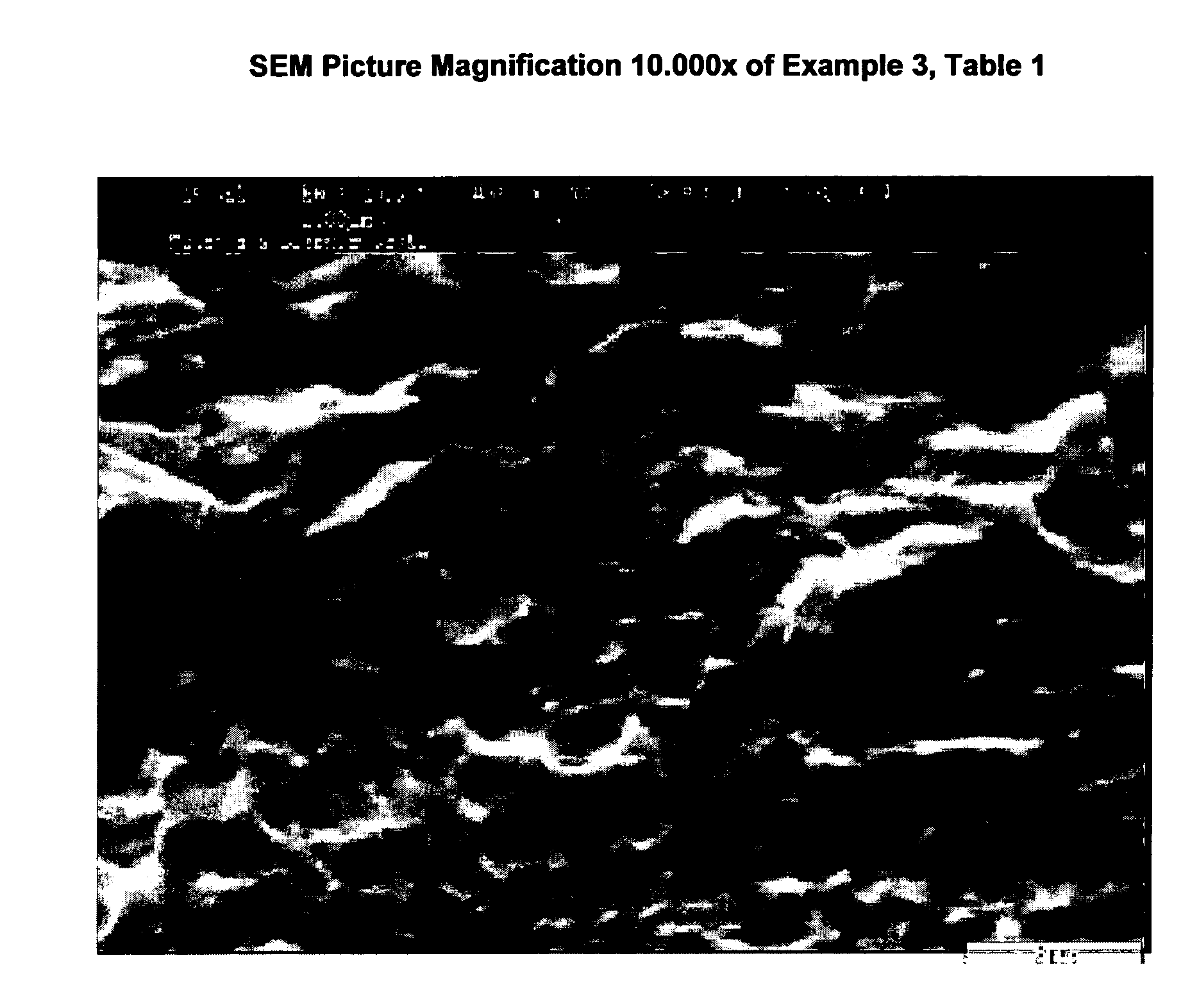
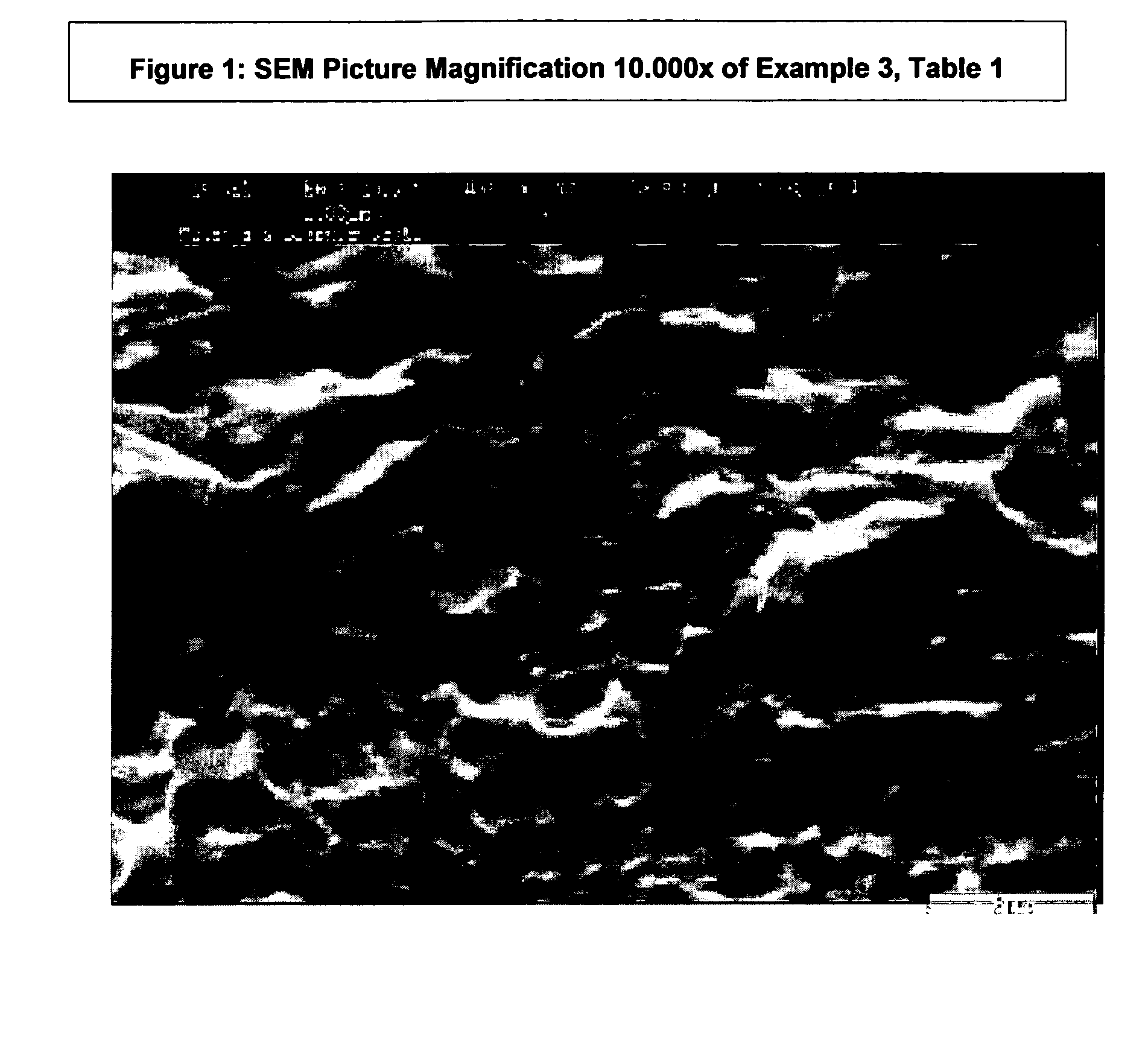
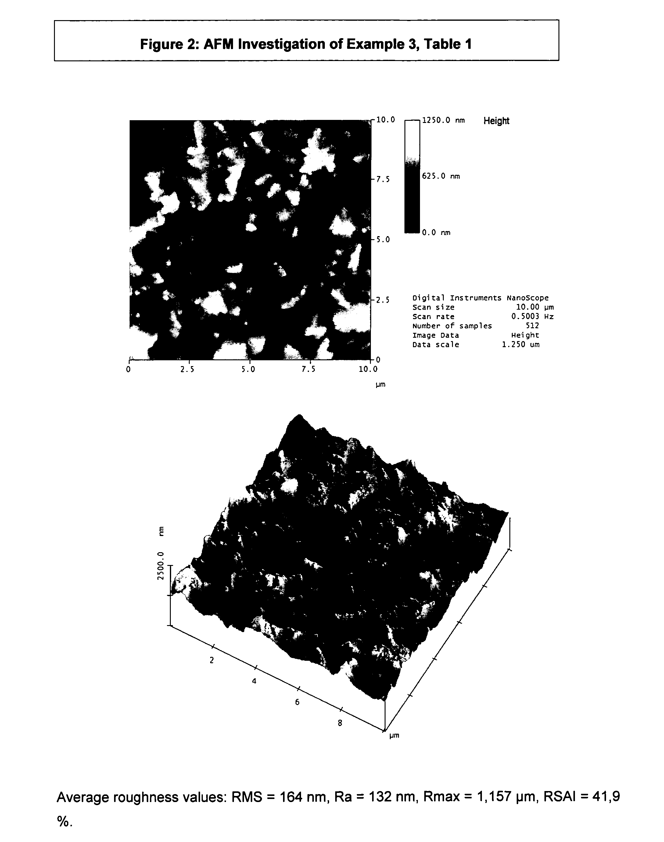
[0046]After roughening the samples with the solution according to the invention (see Table 1 for details) they were coated with a solder mask. An Elpemer SD 2467 DG solder mask was applied with a semi-automatic screen printer. The coated samples were pre-cured for 40 minutes at 80° C.

[0047]A test pattern (Test Coupon G of IPC-2221) was created by using a UV exposure (Stouffer Step 11-12) followed by an aqueous alkaline image development in a 1% sodium carbonate solution at 30° C. in a spray module.

[0048]The test samples were rinsed with city water and finally rinsed with DI water. Afterwards the panels were dried and the final cure was done at 150° C. for 60 minutes. After the final cure the test samples were cut in half and treated either in an immersion tin process for 10 min at 65° C. (commercially available Stannatech process from Atotech Deutschland GmbH) or an electroless nickel-gold process (commercially available Aurotech process from Atotech Deutschland GmbH) consisting of ...


PUM

PropertyMeasurementUnit
Temperatureaaaaaaaaaa
Timeaaaaaaaaaa
Timeaaaaaaaaaa

Abstract

The present invention relates to a method for treating copper or copper alloy surfaces for tight bonding to polymeric substrates, for example solder masks found in multilayer printed circuit boards. The substrate generally is a semiconductor-device, a lead frame or a printed circuit board.

Description

DESCRIPTION OF THE INVENTION[0001]The present invention relates to a method for treating copper or copper alloy surfaces for tight bonding to polymeric substrates, for example solder masks found in multilayer printed circuit boards. The substrate generally is a semiconductor-device, a lead frame or a printed circuit board.BACKGROUND OF THE INVENTION[0002]In manufacturing substrates like printed circuit boards, various steps are carried out in which copper or copper alloy surfaces must be tightly bonded to a polymeric substrate. In some cases, the required adhesion of the formed bonds must be ensured over a long period. In other cases, a tight bond only has to exist for a short period, e.g. when the polymeric substrate only remains on the copper or copper alloy surfaces during manufacture of the printed circuit board. For example, the tight bond of dry film resists (for structuring conductor lines on printed circuit boards) to the copper surfaces only has to exist while manufacturing...

Claims


Application Information

Patent Timeline
IPC IPC(8): H01L21/306C09K13/00
CPCC23F1/18C23F1/46C23F3/06H05K2203/124H05K3/383H05K2203/0796C23G1/103B05D1/02C09K13/00C23F1/02H01L21/302H05K3/0017
Inventor TEWS, DIRKSPARING, CHRISTIAN
Owner ATOTECH DEUT GMBH
Why Eureka
Try Eureka