Barrier layer disposed between a substrate and a transparent conductive oxide layer for thin film silicon solar cells

a barrier layer and silicon solar cell technology, applied in the field of solar cells, can solve the problems of film peeling or cracking at the interface, solar cell deformation, device stability less than desired, etc., and achieve the effect of improving the interface properties

Inactive Publication Date: 2011-04-21
APPLIED MATERIALS INC
View PDF98 Cites 27 Cited by
  • Summary
  • Abstract
  • Description
  • Claims
  • Application Information

AI Technical Summary

Problems solved by technology

It has been found that the properties of thin film solar cells degrade over time upon exposure to light, which can cause the device stability to be less than desired.
Poor nucleation or adhesion of the TCO film formed on the substrate may result in film peeling or cracking at the interface, high contact resistance, and poor optical and electrical film properties.
Furthermore, non-uniform grain growth may result in small random grains formed in the initial stage of the TCO film deposition process, thereby increasing the likelihood of forming defects and pinholes at the interface between the TCO film layer and the substrate, which may adversely affect the optical and electrical properties of the formed TCO film layer.

Method used


Image

  • Barrier layer disposed between a substrate and a transparent conductive oxide layer for thin film silicon solar cells
  • Barrier layer disposed between a substrate and a transparent conductive oxide layer for thin film silicon solar cells
  • Barrier layer disposed between a substrate and a transparent conductive oxide layer for thin film silicon solar cells

Examples


Embodiment Construction

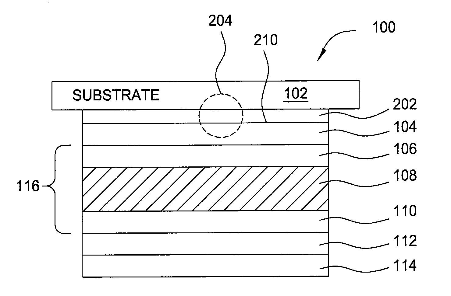
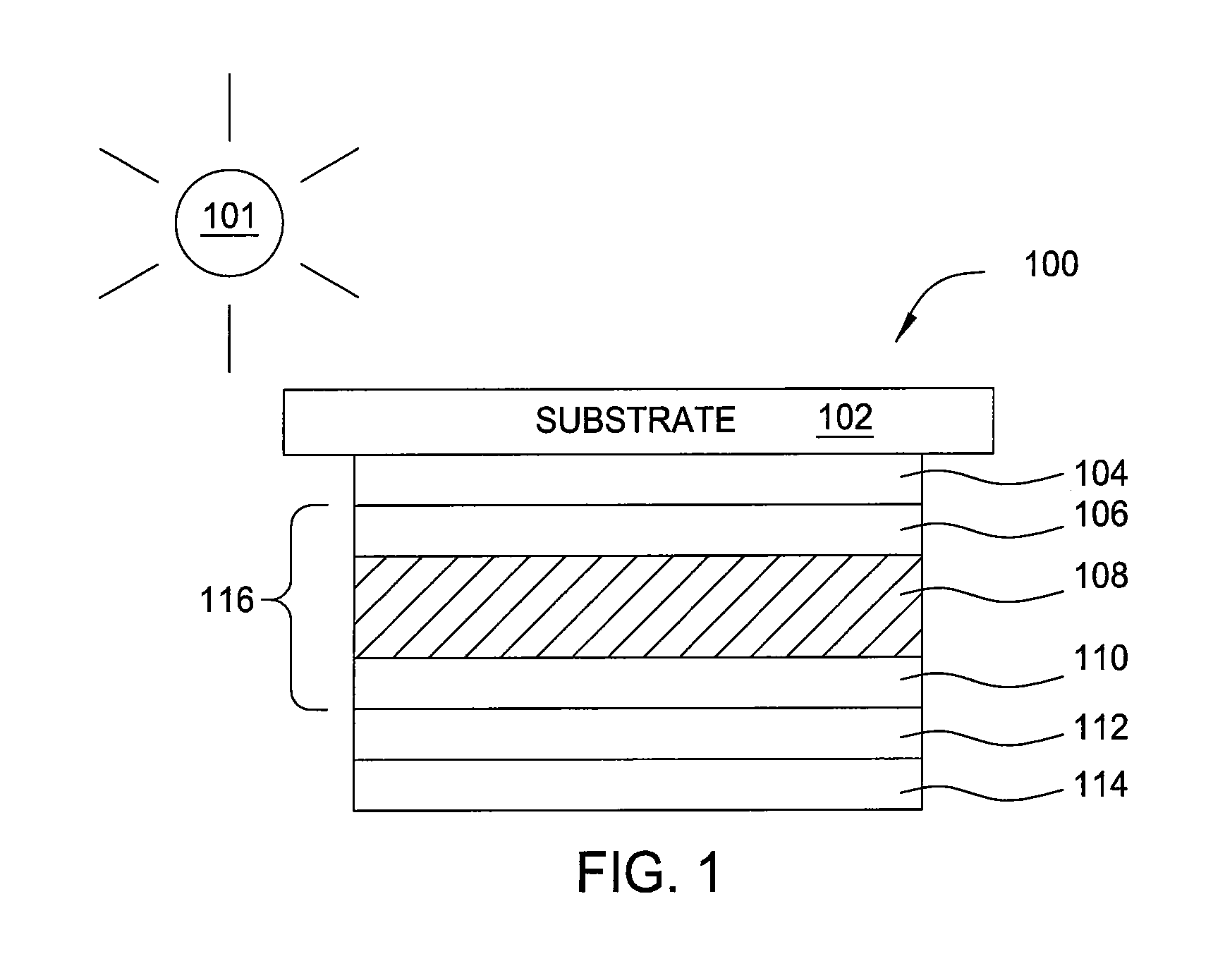
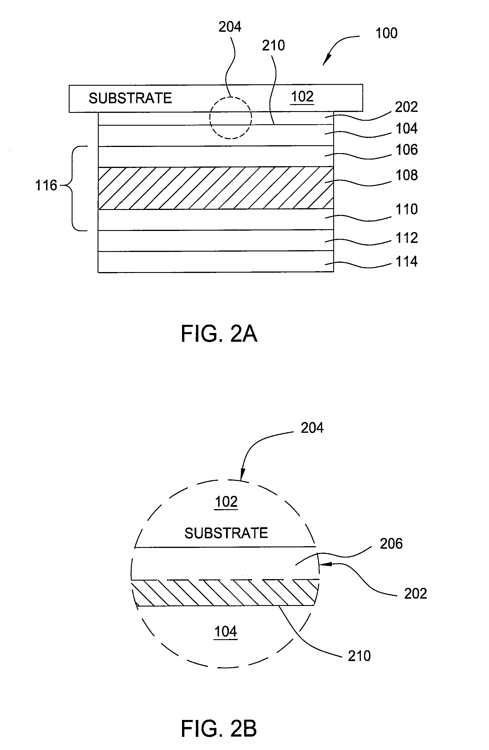
[0021]Thin-film solar cells are generally formed from numerous types of films, or layers, put together in many different ways. Most films used in such devices incorporate a semiconductor element that may comprise silicon, germanium, carbon, boron, phosphorous, nitrogen, oxygen, hydrogen and the like. Characteristics of the different films include degrees of crystallinity, dopant type, dopant concentration, film refractive index, film extinction coefficient, film transparency, film absorption, conductivity, thickness and roughness. Most of these films can be formed by use of a chemical vapor deposition process, which may include some degree of ionization or plasma formation.

[0022]Charge generation during a photovoltaic process is generally provided by a bulk semiconductor layer, such as a silicon containing layer. The bulk layer is also sometimes called an intrinsic layer to distinguish it from the various doped layers present in the solar cell. The intrinsic layer may have any desir...


PUM


Abstract

A method and apparatus for forming solar cells is provided. In one embodiment, a photovoltaic device includes a barrier layer disposed on a substrate, a TCO layer disposed on the barrier layer, and a p-i-n junction cell formed on the TCO layer. In another embodiment, a method for forming a photovoltaic device includes providing a substrate having a surface, forming a barrier layer on the surface of the substrate, forming a TCO layer on a top surface of the barrier layer, and forming a p-i-n junction cell on the TCO layer.

Description

CROSS-REFERENCE TO RELATED APPLICATIONS[0001]This application claims benefit of U.S. Provisional Application Ser. No. 61 / 251,995 filed Oct. 15, 2009 (Attorney Docket No. APPM / 14449L), which is incorporated by reference in their entirety.BACKGROUND OF THE INVENTION[0002]1. Field of the Invention[0003]Embodiments of the present invention generally relate to solar cells and methods for forming the same. More particularly, embodiments of the present invention relate to a barrier layer disposed between a substrate and a transparent conductive oxide (TCO) film layer in thin film solar cell applications.[0004]2. Description of the Related Art[0005]Solar cells convert solar radiation and other light into usable electrical energy. The energy conversion occurs as the result of the photovoltaic effect. Solar cells may be formed from crystalline material or from amorphous or micro-crystalline materials. Generally, there are two major types of solar cells that are produced in large quantities to...

Claims


Application Information

Patent Timeline
Patent Type & Authority Applications(United States)
IPC IPC(8): H01L31/0248H01L31/0224H01L31/075
CPCH01L31/03921H01L31/075Y02E10/547H01L31/1884Y02E10/548H01L31/1804Y02P70/50
Inventor SINGH, KAUSHAL K.PINGALAY, DEEPAKSHRAUTI, SURESH
Owner APPLIED MATERIALS INC
Why Eureka
Try Eureka