Substrate with transparent conductive oxide film, process for its production and photoelectric conversion element

a technology of conductive oxide film and substrate, which is applied in the direction of oxide conductors, non-metal conductors, instruments, etc., can solve the problems of difficult to increase the efficiency of photoelectric conversion, the inability to avoid free electron absorption, and the inability to increase the photoelectric conversion efficiency of solar cells

Inactive Publication Date: 2005-01-06
ASAHI GLASS CO LTD
View PDF8 Cites 82 Cited by
  • Summary
  • Abstract
  • Description
  • Claims
  • Application Information

AI Technical Summary

Problems solved by technology

Consequently, even if light scattering on a long wavelength side is increased by increasing the surface roughness, light absorption of a long wavelength will also increase, whereby as a whole, the photoelectric conversion efficiency of the solar cell will not increase, and it has been difficult to increase the efficiency of the photoelectric conversion by means of a transparent conductive film having a high spectral haze value (which may hereinafter be referred to simply as “a haze”).
However, with the electrode structure disclosed in Examples, both the first and second layers are transparent conductive films, whereby absorption by free electrons can not be avoided.
Accordingly, attenuation of light before reaching the photoelectric conversion layer can not be avoided.
Thus, it has been found that with the construction of the substrate as disclosed in JP-A-3-125481, no significant improvement can be obtained in the photoelectric conversion efficiency.
However, it has been found that also this transparent electrode substrate has a drawback that, like the above-mentioned problem, as light will pass through absorptive two layers of transparent conductive films (continuous films), the amount of incident light to the photoelectric conversion layer will be reduced by an amount absorbed by the conductive films, whereby the photoelectric conversion efficiency will not be improved.
However, this system requires to carry out chemical etching treatment after forming the transparent electrode films and to sufficiently clean and dry the substrate in order to remove the etching solution and then to form the photoelectric conversion layer, whereby the process tends to be cumbersome, and there is a problem that the productivity is low.
However, the means to realize the surface roughness in this process is chemical etching like in the above-mentioned cases, whereby the process tends to be cumbersome, and there will be a problem in mass production.

Method used


Image

  • Substrate with transparent conductive oxide film, process for its production and photoelectric conversion element
  • Substrate with transparent conductive oxide film, process for its production and photoelectric conversion element
  • Substrate with transparent conductive oxide film, process for its production and photoelectric conversion element

Examples


examples

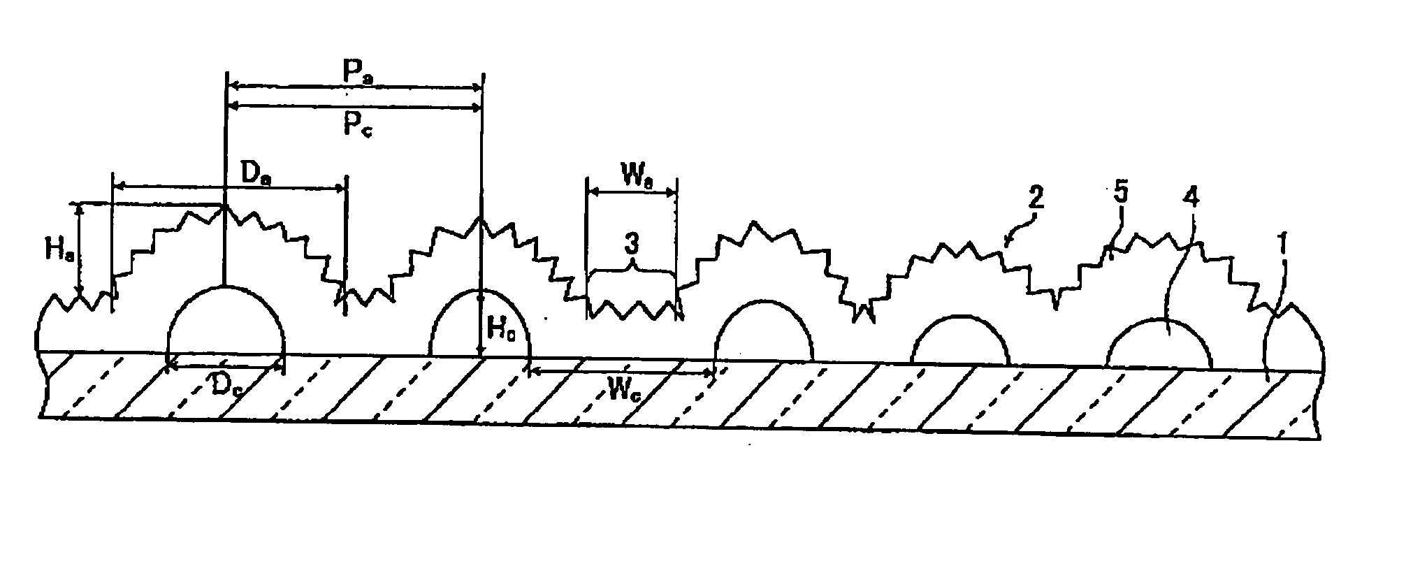
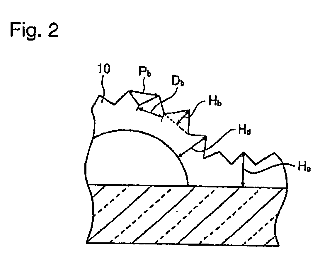
[0161] A substrate with a transparent conductive oxide film of the present invention having a double texture structure was prepared under the conditions as identified in the following Examples.

(1) Production Example 1

Formation of First Oxide

a) EXAMPLE

[0162] A substrate with a transparent conductive oxide film was prepared by an atmospheric pressure Cvn method on a soda lime glass substrate. A soda lime glass substrate of 300 mm×300 mm×1.1 mm in thickness was heated to 500° C. in a belt conveyor furnace (speed of the belt: 1 mr / min), and firstly, 4 L / min of nitrogen gas containing 5 mol % of silane gas and 20 L / min of oxygen gas were blown thereto simultaneously to form a silica film. Then, the glass substrate with this silica film was heated to 540° C., and tin tetrachloride, water and hydrogen chloride gas were simultaneously blown thereto to form SnO2 as the first oxide. Tin tetrachloride was preliminarily heated to 45° C. and transferred onto the substrate by blowing nitrogen...


PUM

PropertyMeasurementUnit
heightaaaaaaaaaa
hazeaaaaaaaaaa
hazeaaaaaaaaaa

Abstract

A substrate with a transparent conductive oxide film (especially a substrate with a transparent conductive oxide film useful as a substrate for a thin-film silicon-based solar cell) being excellent in mass production efficiency and being characterized by having a low resistance, a high transparency and a good light scattering performance over a full wavelength region (300 nm to 3 μm) of solar ray, a process for its production, and a photoelectric conversion element (especially, solar cell) employing the substrate, are presented. A substrate with a transparent conductive oxide film, comprising a substrate and a transparent conductive oxide layer formed on the substrate and constituted by a plurality of ridges is and a plurality of flat portions, wherein the surfaces of the ridges and the flat portions, have many continuous micron-size protrusions.

Description

TECHNICAL FIELD [0001] The present invention relates to a substrate with a transparent conductive oxide film, a process for its production and a photoelectric conversion element (especially a solar cell) employing the substrate. BACKGROUND ART [0002] Thin-film solar cells being photoelectric conversion elements may, for example, be of an amorphous silicon (a-Si) type or a polycrystalline silicon type. In such thin-film silicon type solar cells, a transparent conductive oxide film is used as an incident light side electrode. Such a transparent conductive oxide film is required to have a low resistance and high transparency and to have a high light scattering performance in order to increase the photoelectric conversion efficiency. JP-B-7-105166 discloses a fluorine-doped SnO2 film which contains fluorine in an amount of from 0.01 to 4 mol % based on SnO2 and which has a conductive electron density of from 5×10¹⁹ to 4×1020 cm−3, and the film has a low absorbance, is highly transparent...

Claims


Application Information

Patent Timeline
Patent Type & Authority Applications(United States)
IPC IPC(8): C23C16/40H01L31/0224H01L31/0236H01L31/18
CPCC23C16/0272C23C16/04C23C16/407H01L31/022466H01L31/0236Y10T428/265Y02E10/50Y10T428/263Y10T428/24364Y10T428/261H01L31/1884H01L31/022483H01L31/02363H01L31/02366
Inventor SATO, KAZUOTANEDA, NAOKIFUKAWA, MAKOTOAOMINE, NOBUTAKAKAMBE, MIKA
Owner ASAHI GLASS CO LTD
Why Eureka
Try Eureka