Eureka AIR delivers breakthrough ideas for toughest innovation challenges, trusted by R&D personnel around the world.

Laser annealing method and apparatus

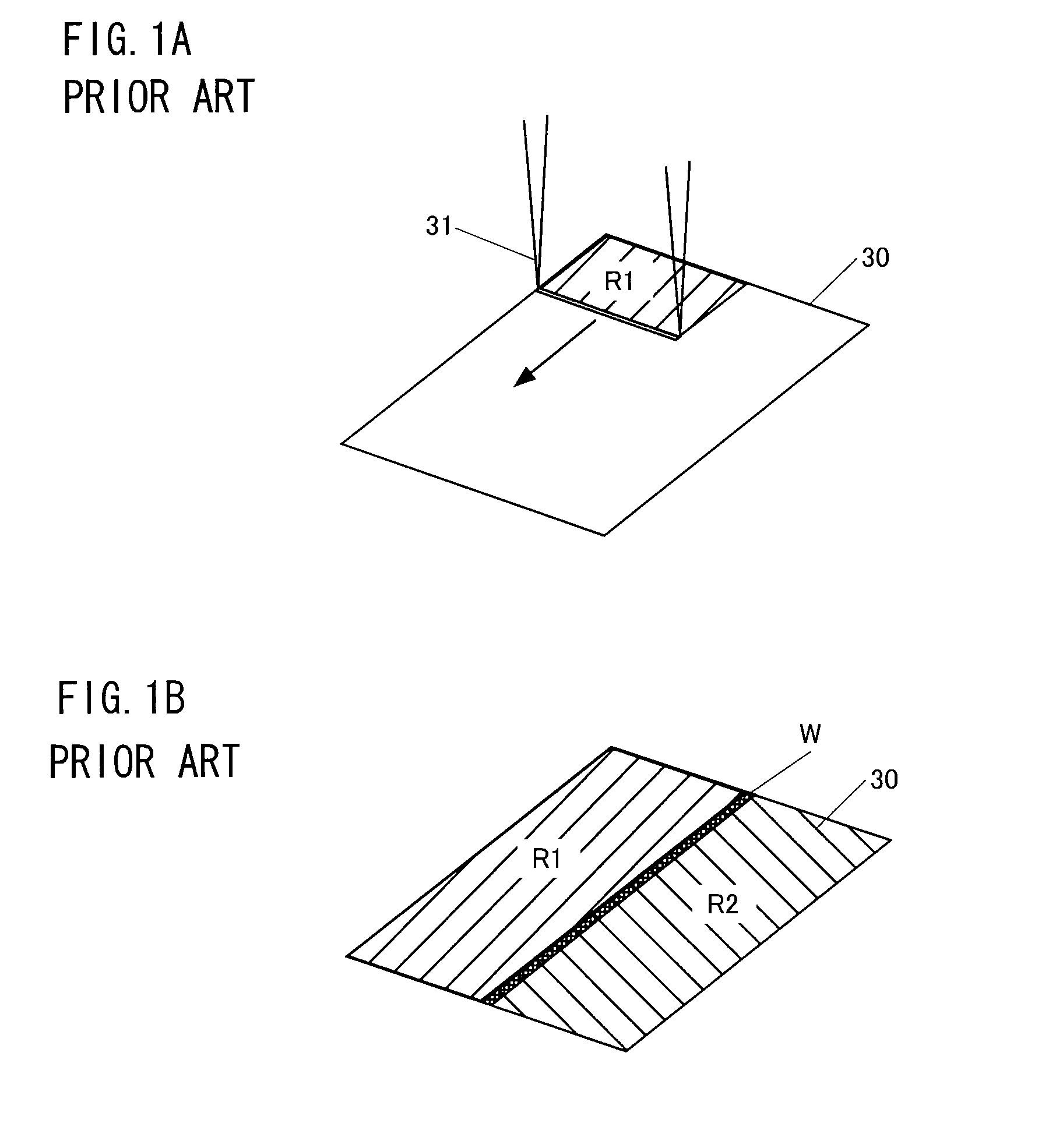
a laser annealing and annealing method technology, applied in the direction of polycrystalline material growth, crystal growth process, manufacturing tools, etc., can solve the problems of insufficient overlap at the edges of the beam, inability to obtain a uniform performance of thin film transistors, and difficulty in manufacturing large-scale displays whose size exceeds 20 inches, so as to prevent a deficit of overlap, reduce non-uniform crystallinity, and suppress excess overlap

Active Publication Date: 2011-04-28
IHI CORP
View PDF41 Cites 3 Cited by
  • Summary
  • Abstract
  • Description
  • Claims
  • Application Information

AI Technical Summary

Benefits of technology

According to the method as set forth in (1) and the apparatus as set forth in (3), since portions corresponding to the edges of the linear beam are shielded by the mask, and the mask is operated so as to periodically Increase and decrease the amount of shielding, the overlap ratio at the shielded beam edge portion is lower than that at the non-shielded portion. In this way, it is possible to suppress an excess of the overlap at the seam portion and prevent a deficit of the overlap by irradiating the beams so as to overlap each other at adjacent rows. Therefore, it is possible to reduce non-uniformity of the crystallinity at the seam portion and form the semiconductor thin film having high uniformity on the entire surface of the substrate.
According to the method as set forth in (3) and the apparatus as set forth in (6), since the piezoelectric element is able to generate a high-frequency oscillation by controlling an application voltage, it is possible to easily realize a fast oscillation of the mask and easily control the overlap ratio.

Problems solved by technology

On the other hand, when there is a small or no overlap of the beams of adjacent rows, the overlap becomes insufficient at the edges of the beams.
When a thin film transistor is manufactured using an area in which the crystallinity is not uniform, it is not possible to obtain a uniform performance of the thin film transistor.
In the case of a green YAG laser, since the beam length thereof is short, it is difficult to manufacture a large-size display whose size exceeds 20 inches.
However, the method of Patent Document 1 has a problem in that it is not easy to regulate the width dimension and the energy density of the laser light, and productivity of the device decreases.

Method used


Image

  • Laser annealing method and apparatus
  • Laser annealing method and apparatus
  • Laser annealing method and apparatus

Examples


Embodiment Construction

Preferred embodiments of the present invention will be described below in detail with reference to the accompanying drawings. Same reference numerals are given to common portions in each of the drawings to avoid redundant description.

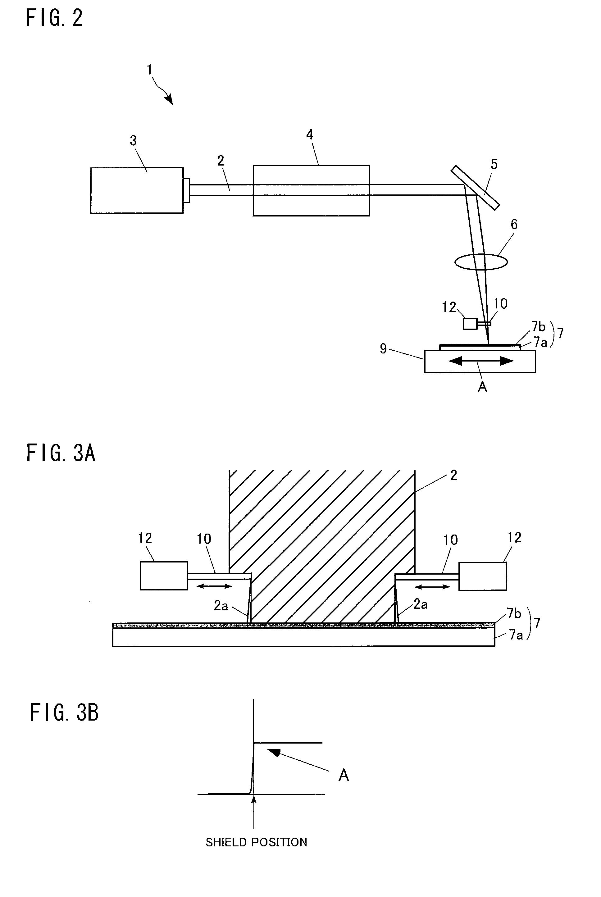
FIG. 2 is a diagram showing an entire configuration of a laser annealing apparatus 1 according to an embodiment of the present invention.

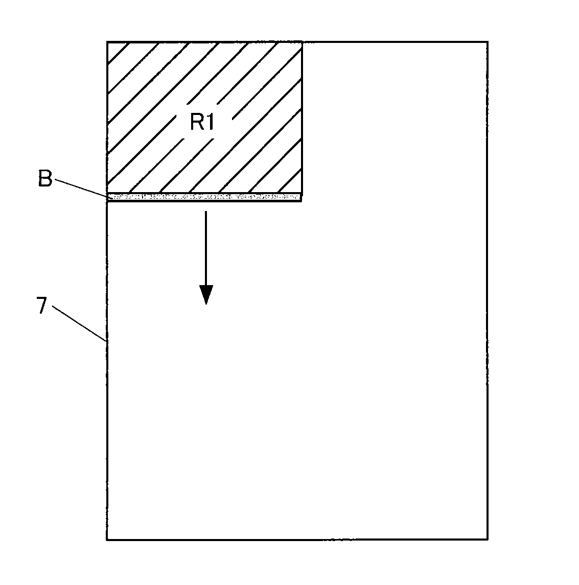
The laser annealing apparatus 1 includes, as its basic constituent elements, a laser light source 3 that emits laser light 2, a beam shaping optical system 4 that shapes the laser light 2 from the laser light source 3, a reflecting mirror 5 that reflects the laser light 2 towards a workpiece 7, a condensing lens 6 that condenses the laser light 2 from the reflecting mirror 5 onto the surface of the workpiece 7, and a movable stage 9 that moves while carrying the workpiece 7.

As the laser light source 3, an excimer laser, a solid-state laser, or a semiconductor laser can be used, for example. As examples of the solid-sta...


PUM

PropertyMeasurementUnit
lengthaaaaaaaaaa
lengthaaaaaaaaaa
lengthaaaaaaaaaa

Abstract

Disclosed are a laser annealing method and apparatus capable of forming a crystalline semiconductor thin film on the entire surface of a substrate without sacrificing the uniformity of crystallinity in a seam portion in a long-axis direction of laser light, the crystalline semiconductor thin film having good properties and high uniformity to an extent that the seam portion is not visually recognizable.During the irradiation of a linear beam, portions corresponding to the edges of the linear beam are shielded by a mask 10 which is disposed on the optical path of a laser light 2, and the mask 10 is operated so that the amount of shielding is periodically increased and decreased.

Description

BACKGROUND OF THE INVENTION1. Technical Field of the InventionThe present invention relates to a laser annealing method and apparatus for performing an annealing treatment on a workpiece to be processed by irradiating the workpiece with laser light.2. Description of the Related ArtHitherto, in order to realize a high-performance device such as a liquid crystal display, a method of forming a high-performance semiconductor device such as a thin film transistor on an insulating substrate such as a glass substrate has been developed. In this semiconductor device, thin-film polycrystalline silicon obtained by crystallizing amorphous silicon by a heat treatment is generally used.As a method of manufacturing a polycrystalline silicon film, a method of forming an amorphous silicon film in advance on a substrate and crystallizing the film by irradiation of laser light is generally used. According to this method, since it utilizes a crystallization phenomenon in the process of melting and sol...

Claims


Application Information

Patent Timeline
Patent Type & Authority Applications(United States)
IPC IPC(8): H01L21/268B23K26/06
CPCB23K26/0656B23K26/0738C30B29/06C30B1/023H01L21/02678B23K26/066
Inventor KAWAGUCHI, NORIHITOKAWAKAMI, RYUSUKENISHIDA, KENICHIROMASAKI, MIYUKIMORITA, MASARU
Owner IHI CORP
Why Eureka
Eureka Blog
Learn More