Ultra high thermal performance packaging for optoelectronics devices

Active Publication Date: 2011-05-05
LUMILEDS HLDG BV
View PDF10 Cites 48 Cited by
  • Summary
  • Abstract
  • Description
  • Claims
  • Application Information

AI Technical Summary

Benefits of technology

[0044]As the electro-deposition or electroplating process is usually carried out at low temperature (less than 100 degrees Celsius), mismatches in thermal expansion of materials used in the package construction are minimised and do not result in stress in the package associated with solder processes. The present invention allows the thermal resistance from the LED junction to the heat spreader t

Problems solved by technology

This reason for this is the inherent conflict arising between thermal conductivity and electrical insulation when selecting suitable materials for packaging.
The largest challenges associated with the packaging come from electrically pumped light emitting devices.
The conversion from electrical energy to light photons out dictates that the associated wall plug efficiency of the device is never unity, thereby introducing substantial heating in the vicinity of the small format device.
These comprise of a chip level small format device and are typically driven at high drive currents resulting in high power densities generated inside the material causing local heating effects.
However, if this type of IMS-PCB is used with the LED placed directly on the PCB, then high junction temperatures will occur, as the thermal load will not be able to spread adequately in layer 103.
Of course, all these layers of packaging create extra cost and extra interfaces that increase thermal resistance.
This is an important issue, if typical metal, graphite or conductive plastic heat sinks are used to prevent the h

Method used


Image

  • Ultra high thermal performance packaging for optoelectronics devices
  • Ultra high thermal performance packaging for optoelectronics devices
  • Ultra high thermal performance packaging for optoelectronics devices

Examples


Example

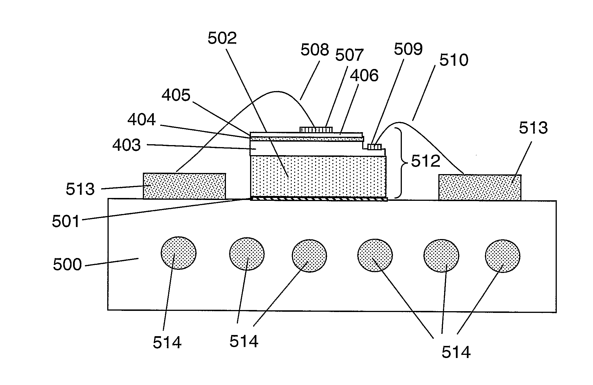
[0055]Heat is a form of energy that is related to vibration at the molecular level, and is a by product of many processes. In the case of LEDs, this includes the recombination of photons in a semiconductor bandgap. Since LEDs and many other electronic components are sensitive to heat, it is important to remove excess heat that will adversely impact performance. In traditional light sources, such as incandescent lights, only a small proportion of the electrical energy is actually converted to useful light. The majority of the energy is converted to heat that must be removed from the light source. The heat energy may be transferred in one of three ways, namely by conduction, convection or radiation.

[0056]Conduction is the method in which heat energy is transferred between two objects that are in contact with one another. Convection is the process by which heat is transferred through the movement of gas or liquid from an area of higher temperature to one of lower temperature. Hot air r...


PUM

PropertyMeasurementUnit
Fractionaaaaaaaaaa
Thicknessaaaaaaaaaa
Thicknessaaaaaaaaaa

Abstract

A light emitting module comprises a light emitting device (LED) mounted on a high thermal dissipation sub-mount, which performs the traditionally function of heat spread and the first part of the heat sinking. The sub-mount is a grown metal that is formed by an electroplating, electroforming, electrodeposition or electroless plating process, thereby minimising thermal resistance at this stage. An electrically insulating and thermally conducting layer is at least partially disposed across the interface between the grown semiconductor layers of the light emitting device and the formed metal layers of the sub-mount to further improve the electrical isolation of the light emitting device from the grown sub-mount. The top surface of the LED is protected from electroplating or electroforming by a wax or polymer or other removable material on a temporary substrate, mould or mandrel, which can be removed after plating, thereby releasing the LED module for subsequent processing.

Description

FIELD OF THE INVENTION[0001]The present invention relates to an improved module and packaging technique providing high thermal performance for light emitting devices, particularly Light Emitting Diodes (LEDs).BACKGROUND TO THE INVENTION[0002]There are many types of packages used to manage the thermal, optical and electrical connections to small optoelectronic devices. This reason for this is the inherent conflict arising between thermal conductivity and electrical insulation when selecting suitable materials for packaging. Typical Optoelectronic devices include lasers, LEDs, detectors and photovoltaic devices. The largest challenges associated with the packaging come from electrically pumped light emitting devices. The conversion from electrical energy to light photons out dictates that the associated wall plug efficiency of the device is never unity, thereby introducing substantial heating in the vicinity of the small format device.[0003]Of particular interest to the present invent...

Claims


Application Information

Patent Timeline
IPC IPC(8): H01L33/10H01L33/64H01L33/48H01L33/20
CPCC23C18/1657C23C28/00H01L2924/19107C25D5/34H01L33/20H01L33/641H01L33/642C23C28/322C23C28/34C23C28/341C23C28/343C23C28/345H01L2224/45147H01L2924/01047H01L2924/01015H01L2224/48091H01L2224/49107H01L2224/73265H01L2924/00014H01L2924/00H01L2924/00011H01L2924/10252H01L2924/10253H01L2924/10272H01L2924/181H01L2224/32225H01L2224/48227H01L2924/01004H01L2924/00012
Inventor MCKENZIE, JAMES STUARTZOOROB, MAJD
Owner LUMILEDS HLDG BV
Why Eureka
Try Eureka