

Liquid crystal display device, driving method of the same, and electronic appliance including the same
a technology of liquid crystal display and driving method, which is applied in the direction of semiconductor devices, instruments, optics, etc., can solve the problems that the transistor is not always suitable for being formed over a larger glass substrate, and achieve the effect of reducing off-state current and low power consumption
- Summary
- Abstract
- Description
- Claims
- Application Information
AI Technical Summary
Benefits of technology
Problems solved by technology
Method used
Image

Examples
embodiment 1
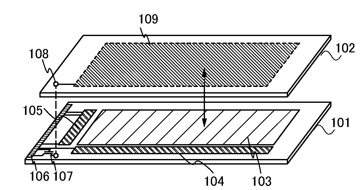
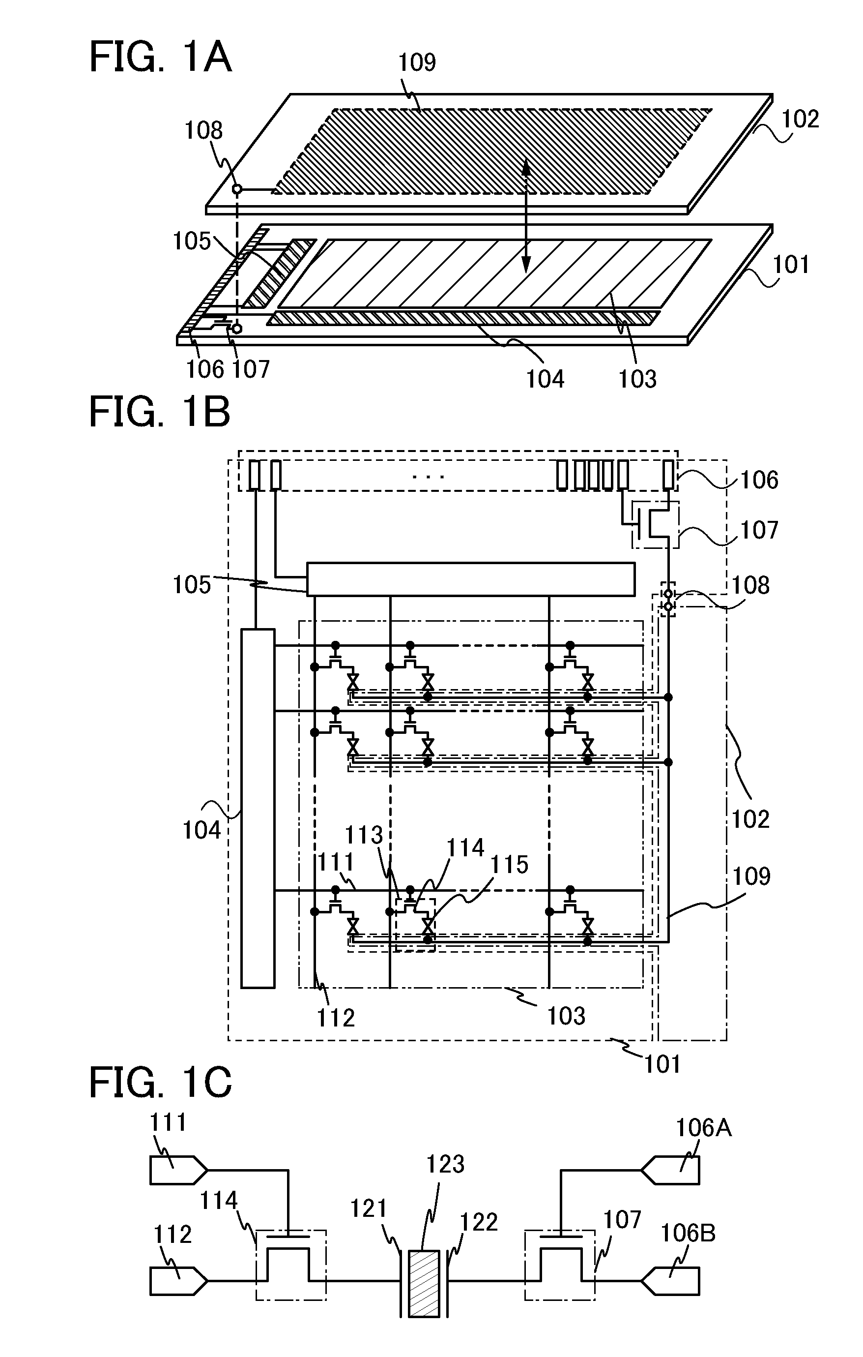
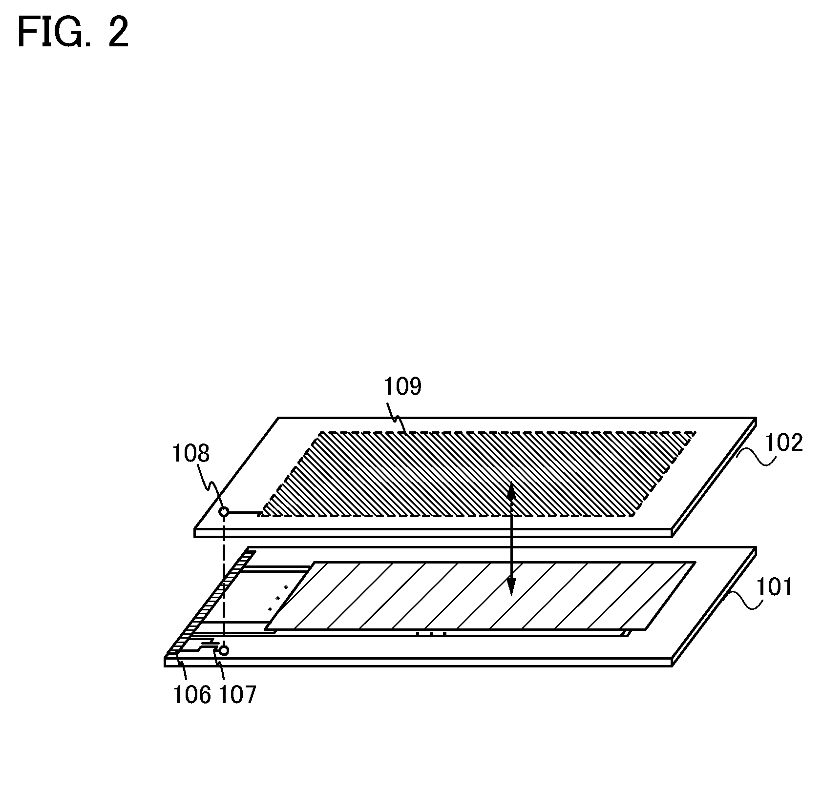
[0038]In this embodiment, a schematic view, circuit diagrams, a timing chart, and the like of a liquid crystal display device are described, and an effect of a structure of this embodiment is described. First, a schematic view of a liquid crystal display device is described with reference to FIG. 1A.
[0039]A liquid crystal display device includes a first substrate 101 and a second substrate 102 as illustrated in FIG. 1A. The first substrate 101 includes a pixel circuit 103, a gate line driver circuit 104, a signal line driver circuit 105, a terminal portion 106, and a switching transistor 107. The second substrate 102 includes a common connection portion 108 (also referred to as a common contact) and a counter electrode 109.
[0040]It is necessary that the first substrate 101 and the second substrate 102 have enough heat resistance to withstand heat treatment to be performed later. Further, it is necessary that at least one of the first substrate and the second substrate have a light-t...
embodiment 2
[0092]A structure of the liquid crystal display device in Embodiment 1 is described with reference to a specific top view and cross-sectional views in FIGS. 4A to 4C.
[0093]FIG. 4A is a top view of a liquid crystal display device of the present invention. FIG. 4A is a top view of a liquid crystal display device in which a flexible printed circuit, an FPC, has not been attached to a first substrate 1210. FIG. 4B is a cross-sectional view taken along line G-H of FIG. 4A, which shows a connection region of a conductive particle and a connection wiring. FIG. 4C is a cross-sectional view taken along line E-F of FIG. 4A, which shows a connection region of a pixel circuit and a connection wiring.
[0094]Although FIGS. 4A to 4C illustrate an example of a transmissive liquid crystal display device, this embodiment is applicable to a transflective liquid crystal display device and a reflective liquid crystal display device.
[0095]The first substrate 1210 which is provided with pixel electrodes, w...
embodiment 3
[0125]In this embodiment, an example of thin film transistors applicable to a liquid crystal display device disclosed in this specification is described. A thin film transistor 410 and a thin film transistor 420 to be described in this embodiment can be used as the switching transistor 1261 and the pixel transistor 1211 in Embodiment 2, respectively.
[0126]An embodiment of a liquid crystal display device of this embodiment and a manufacturing method of the liquid crystal display device is described with reference to FIGS. 5A to 5E.
[0127]FIGS. 5A to 5E illustrate an example of a cross-sectional structure of a liquid crystal display device. The thin film transistors 410 and 420 in FIGS. 5A to 5E each have a kind of bottom-gate structure called a channel-etched type and are also referred to as inverted-staggered thin film transistors. In FIGS. 5A to 5E, the thin film transistor 410 is a switching transistor and the thin film transistor 420 is a pixel transistor.
[0128]Although descriptio...
PUM
| Property | Measurement | Unit |
|---|---|---|
| thickness | aaaaa | aaaaa |
| threshold voltage | aaaaa | aaaaa |
| energy gap | aaaaa | aaaaa |
Abstract
Description
Claims
Application Information