Superluminescent diodes by crystallographic etching

a crystallographic etching and superluminescent diode technology, applied in the direction of lasers, semiconductor devices, semiconductor lasers, etc., can solve the problems of increasing the cost of fabrication, requiring multiple layers of effective anti-reflective coatings, and additional processing steps that are less compatible with mass production, so as to reduce internal loss

Inactive Publication Date: 2011-05-05
RGT UNIV OF CALIFORNIA
View PDF20 Cites 244 Cited by
  • Summary
  • Abstract
  • Description
  • Claims
  • Application Information

AI Technical Summary

Benefits of technology

[0028]The waveguide structure may utilize index guiding or gain guiding to reduce internal loss.
[0029]The present invention further discloses a method of fabricating a nonpolar or semipolar III-Nitride based optoelectronic device, comprising obtaining a first nonpolar or semipolar III-Nitride based optoelectronic device comprising an active region, a waveguide structure to provide optical confinement of light emitted from the active region, and a first facet and a second facet on opposite ends of the waveguide structure, wherein the first facet and the second facet have opposite surface polarity; and roughening a surface of the first facet, thereby fabricating a second nonpolar or semipolar III-Nitride based optoelectronic device.

Problems solved by technology

Passive absorbers require additional wafer real estate, effective anti-reflective coatings require multiple layers and are relatively expensive to fabricate, and angled facets require additional processing steps that are less compatible with mass production than, for example, a batch wet etching technique.

Method used


Image

  • Superluminescent diodes by crystallographic etching
  • Superluminescent diodes by crystallographic etching
  • Superluminescent diodes by crystallographic etching

Examples


Embodiment Construction

[0041]In the following description of the preferred embodiment, reference is made to the accompanying drawings which form a part hereof, and in which is shown by way of illustration a specific embodiment in which the invention may be practiced. It is to be understood that other embodiments may be utilized and structural changes may be made without departing from the scope of the present invention.

OVERVIEW

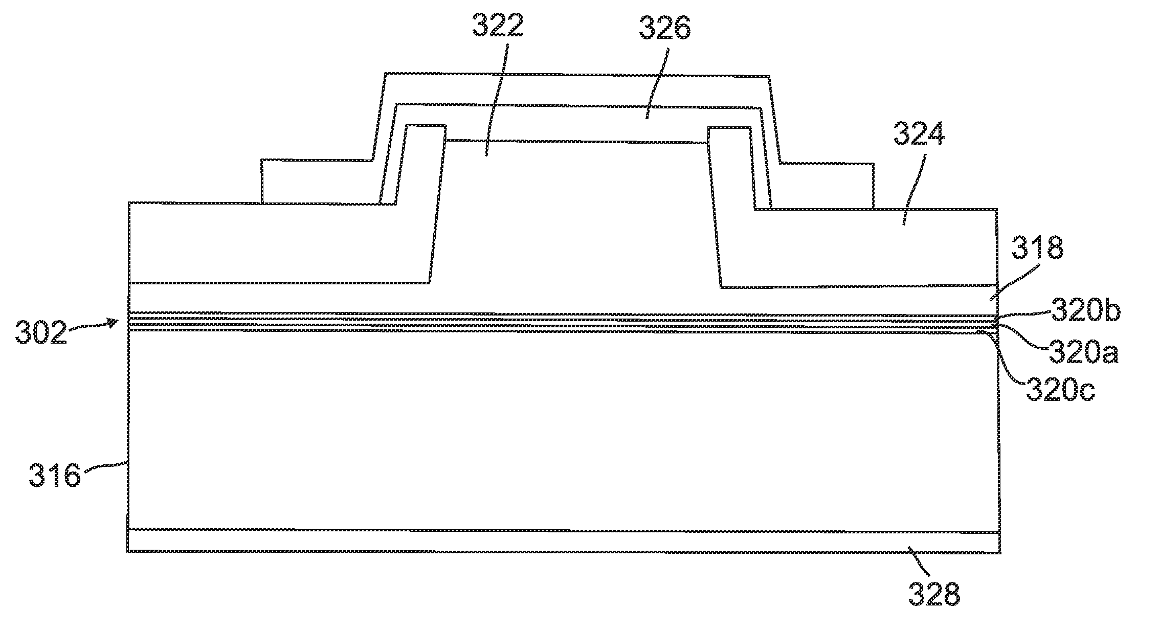
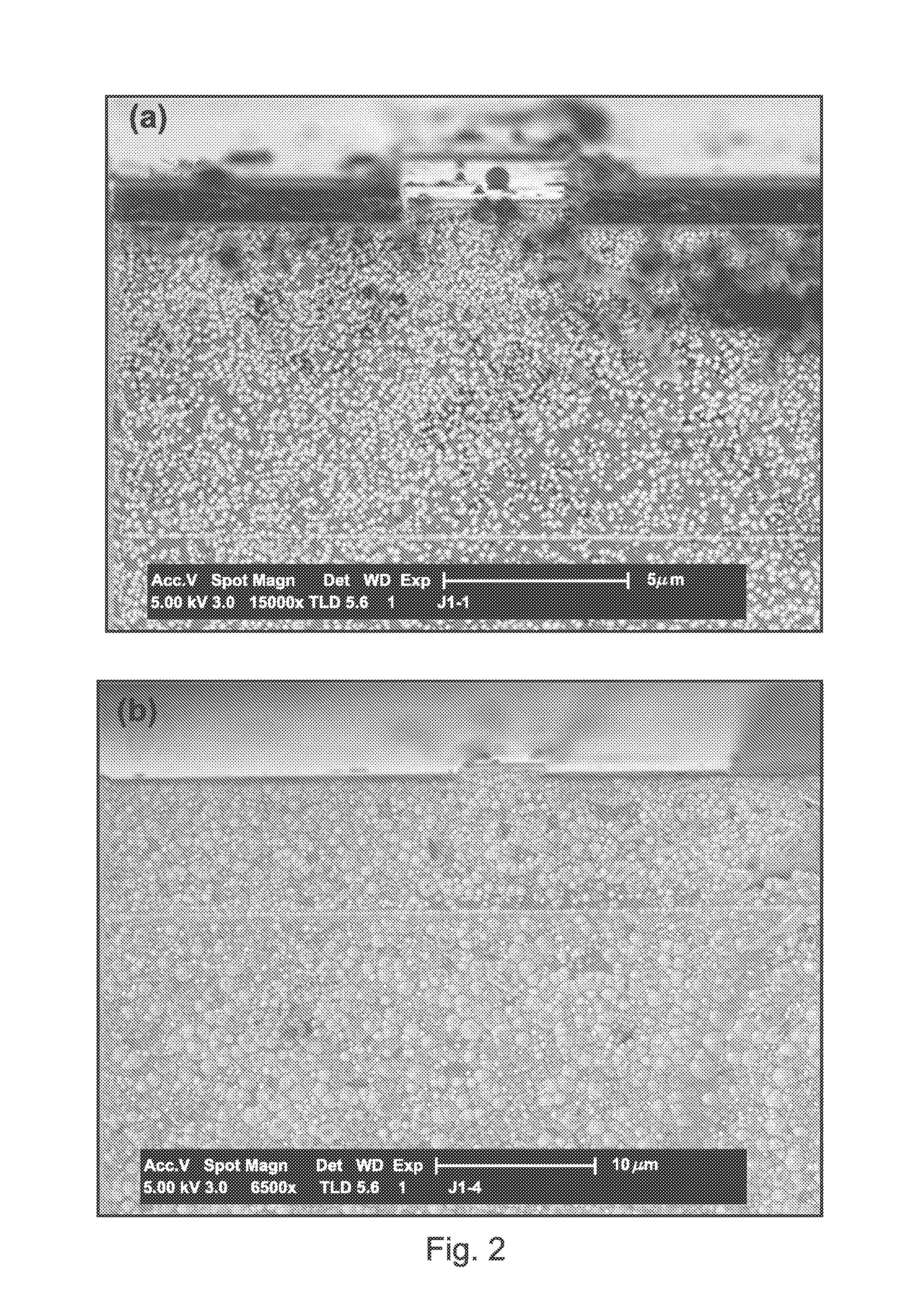
[0042]Crystallographic etching to form hexagonal pyramids has been demonstrated on the c− facet of m-plane (In, Al, Ga)N, and SLD device fabrication has been demonstrated. This invention allows the fabrication of a low reflectance facet suitable for production of nonpolar (Ga,In,Al,B)N based SLDs.

[0043]In one embodiment of the present invention, the non-reflecting −c plane facet, intended to prevent optical feedback along the c-axis waveguide, was fabricated by KOH wet etching. KOH selectively etched the cleaved −c facet leading to the formation of hexagonal pyramids without etching...


PUM


Abstract

An optoelectronic device, comprising an active region and a waveguide structure to provide optical confinement of light emitted from the active region; a pair of facets on opposite ends of the device, having opposite surface polarity; and one of the facets which has been roughened by a crystallographic chemical etching process, wherein the device is a nonpolar or semipolar (Ga,In,Al,B)N based device.

Description

CROSS REFERENCE TO RELATED APPLICATIONS[0001]This application claims priority under 35 U.S.C. §119(e) to co-pending and commonly-assigned U.S. Provisional Patent Application Ser. No. 61 / 257,752 entitled “SUPERLUMINESCENT DIODES BY CRYSTALLOGRAPHIC ETCHING,” filed on Nov. 3, 2009, by Matthew T. Hardy, You-da Lin, Hiroaki Ohta, Steven P. DenBaars, James S. Speck, and Shuji Nakamura, attorney's docket number 30794.330-US-P1 (2010-113), which application is incorporated by reference herein.[0002]This application is related to the following co-pending and commonly-assigned U.S. patent applications:[0003]U.S. Utility application Ser. No. 10 / 581,940, filed on Jun. 7, 2006, now U.S. Pat. No. 7,704,763, issued Apr. 27, 2010, by Tetsuo Fujii, Yan Gao, Evelyn. L. Hu, and Shuji Nakamura, entitled “HIGHLY EFFICIENT GALLIUM NITRIDE BASED LIGHT EMITTING DIODES VIA SURFACE ROUGHENING,” attorney's docket number 30794.108-US-WO (2004-063), which application claims the benefit under 35 U.S.C Section 3...

Claims


Application Information

Patent Timeline
Patent Type & Authority Applications(United States)
IPC IPC(8): H01S5/323H01L33/22H01L21/302
CPCB82Y20/00H01L33/0045H01S5/34333H01S5/22H01S5/1082H01L33/16H01L33/22
Inventor HARDY, MATTHEW T.LIN, YOU-DAOHTA, HIROAKIDENBAARS, STEVEN P.SPECK, JAMES S.NAKAMURA, SHUJIKELCHNER, KATHRYN M.
Owner RGT UNIV OF CALIFORNIA
Why Eureka
Try Eureka