Carbon containing low-k dielectric constant recovery using UV treatment

Active Publication Date: 2011-05-19
NOVELLUS SYSTEMS
View PDF100 Cites 78 Cited by
  • Summary
  • Abstract
  • Description
  • Claims
  • Application Information

AI Technical Summary

Benefits of technology

[0010]The present invention provides a method for treatment of carbon-containing low-k dielectric with ultraviolet (UV) radiation and/or a chemical silylating agent, for the repair of process-induced dielectric damage. The carbon-containing low-k dielectric may be, but is not limited to, carbon-doped oxide (CDO) having a dielectric constant of 2.7 or lower, including ultra low-k dielectrics having pre-processing dielectric constants as low as 2.6, 2.5, 2.4 or lower, and possibly including a metal fe

Problems solved by technology

These low-k dielectrics are mechanically weaker than previous generation dielectric materials.
The inherently weak nature of the low-k dielectric material can pose significant challenges for downstream electronic-packaging processes and material compatibility.
This low density introduces a host of process integration and material compatibility difficulties.
Achieving a balance between maintaining a low-k film's integrity, integrating it properly, and performing the necessary stripping, cleaning, and conditioning is challenging.
The properties that give carbon-containing low-k dielectric materials their desirable low dielectric constants are the very same properties that are leading to significant integration challenges.
Because of the mechanical weakness, carbon-containing low-k films are susceptible to kinetic plasma damage that can undesirably densify the film and thus increase the film's effective k value.
The susceptibility of carbon-containing low-k materials to plasma modification poses a

Method used


Image

  • Carbon containing low-k dielectric constant recovery using UV treatment
  • Carbon containing low-k dielectric constant recovery using UV treatment
  • Carbon containing low-k dielectric constant recovery using UV treatment

Examples


examples

[0093]The following provides examples of specific implementations of the present invention and performance data in order to give a better understanding of the operation and benefits of the invention. The invention is, however, in no way limited to these specific implementations.

[0094]Post-CMP k Recovery Using UV Treatment

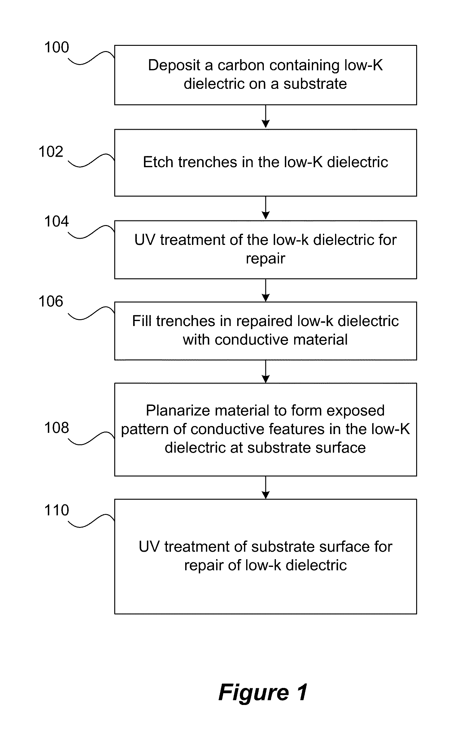
[0095]As part of the solution to lower RC delay, materials with significantly lower k (k<2.60) are being used as ILD materials. The typical way to reduce the k is through incorporation of porogen in these materials, which is eventually driven out and the film is cross-linked to increase its hardness (typically using UV).

[0096]After electroplating of copper, it is planarized using CMP. These porous ULK materials are susceptible to CMP damage. Some amount of C removal occurs from the surface of these films, with consequent moisture intake resulting in an increase in its dielectric constant.

[0097]The next step in the process is deposition of a dielectric barrier / etch s...


PUM


Abstract

A method for the ultraviolet (UV) treatment of carbon-containing low-k dielectric and associated apparatus enables process induced damage repair. The methods of the invention are particularly applicable in the context of damascene processing to recover lost low-k property of a dielectric damaged during processing, either pre-metallization, post-planarization, or both. UV treatments can include an exposure of the subject low-k dielectric to a constrained UV spectral profile and/or chemical silylating agent, or both.

Description

CROSS REFERENCE TO RELATED APPLICATION[0001]This application is a continuation-in-part of prior application Ser. No. 12 / 940,324, filed Nov. 5, 2010 entitled UV TREATMENT FOR CARBON-CONTAINING LOW-K DIELECTRIC REPAIR IN SEMICONDUCTOR PROCESSING, now pending; which is a divisional application of application Ser. No. 11 / 590,661, filed Oct. 30, 2006 entitled UV TREATMENT FOR CARBON-CONTAINING LOW-K DIELECTRIC REPAIR IN SEMICONDUCTOR PROCESSING; the disclosures of which are incorporated by reference herein in their entirety.BACKGROUND OF THE INVENTION[0002]The invention relates to low dielectric constant layers in semiconductor processing for use in various applications. More specifically, the invention relates to the treatment for repair of process-induced damage of low dielectric constant dielectric materials in, for example, damascene processing.[0003]The invention relates to semiconductor processing, in particular to repair of process-induced damage of low dielectric constant dielect...

Claims


Application Information

Patent Timeline
IPC IPC(8): H01L21/268H01L21/306B01J19/12
CPCH01L21/3105H01L21/67115H01L21/76825H01L21/76814H01L21/76813H01L21/26H01L21/31H01L21/324
Inventor VARADARAJAN, BHADRI N.MCLAUGHLIN, KEVIN M.VAN SCHRAVENDIJK, BART
Owner NOVELLUS SYSTEMS
Why Eureka
Try Eureka