Electrophotographic photosensitive member and electrophotographic apparatus

Inactive Publication Date: 2011-05-26
CANON KK
View PDF24 Cites 5 Cited by
  • Summary
  • Abstract
  • Description
  • Claims
  • Application Information

AI Technical Summary

Benefits of technology

[0010]An object of the present invention is to provide a long-life electrophotographic photosensitive member which realizes favorable adhesion even when a sudden environmental change occurs while keeping favorable photosensitive characteristics, even when an a-SiC surface layer with high internal stress is formed on a photoconductive layer.
[0012]However, it has been found out that by reducing the carbon atomic content outside the region with a high hydrogen atomic ratio in the intermediate layer, the characters on the output image sometimes become thin when the image is output with the electrophotographic apparatus. Thus, the present inventors made study in order to realize further improvement in the photosensitive characteristics. As a result, the present inventors have found out that by reducing the carbon atomic ratio of the intermediate layer in the region with a high hydrogen ratio of the intermediate layer, in more detail, by making the region with a high hydrogen atomic ratio the minimum region of the distribution in the layer thickness direction of the carbon atomic ratio, the resistance in the region with a high hydrogen atomic ratio in the intermediate layer can be reduced, and coexistence of enhancement in adhesion and favorable photosensitive characteristics is possible.
[0015]According to the present invention, a long-life electrophotographic photosensitive member can be provided, which realizes favorable adhesion even if a sudden environmental change occurs, while maintaining favorable photosensitive characteristics.

Problems solved by technology

However, when the surface layer is formed on the photoconductive layer to be thick, if a sudden environmental change (sudden change in temperature and humidity) occurs, separation sometimes occurs in the vicinity of the interface between the photoconductive layer and the a-SiC surface layer.
From the above, it is a difficult problem to keep favorable adhesion of the photoconductive layer and the a-SiC surface layer when a sudden environmental change occurs, in case that the a-SiC surface layer with high internal stress is formed on the photoconductive layer in the conventional electrophotographic photosensitive member.

Method used


Image

  • Electrophotographic photosensitive member and electrophotographic apparatus
  • Electrophotographic photosensitive member and electrophotographic apparatus
  • Electrophotographic photosensitive member and electrophotographic apparatus

Examples


experimental example 1

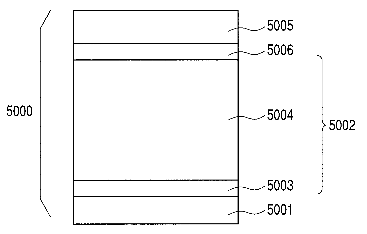
[0079]By using the plasma processing apparatus shown in FIG. 3 using a high-frequency power supply in a RF band as a frequency, a charge injection inhibition layer and a photoconductive layer were formed under the conditions shown in the following Table 1 on the cylindrical substrate (cylindrical aluminum substrate with mirror machining applied of a diameter of 80 mm, a length of 358 mm and a thickness of 3 mm). After the photoconductive layer was formed, a positively chargeable a-Si photosensitive member was produced under the conditions shown in the following Table 4 by using the intermediate layer forming conditions shown in the following Table 2 and the surface layer forming conditions shown in the following Table 3. At this time, with respect to Nos. 1 and 2 of the layer forming conditions of the following Table 4, in a variable layer 1, the layer formation time was regulated so that the layer thickness was 0.20 μm, and the internal pressure and the high-frequency power were se...

example 1

[0094]By using the plasma processing apparatus using a high-frequency power supply in an RF band as a frequency illustrated in FIG. 3 as in experimental example 1, the charge injection inhibition layer and the photoconductive layer were formed on the cylindrical substrate under the conditions shown in the above described Table 1. After the photoconductive layer was formed, the surface layer was formed under the conditions of the layer forming condition No. 3 shown in the above described Table 4, and five positively chargeable a-Si photosensitive members were produced. At this time, the layer thickness of the surface layer was regulated to be 2.00 μm. The intermediate layer forming conditions in the layer forming condition No. 3 shown in the above described Table 4 are shown in the above described Table 2. With respect to the five electrophotographic photosensitive members produced according to example 1, the surface roughness was measured under the conditions which will be described...

example 2

[0118]Similarly to example 1, a plasma processing apparatus using a high-frequency power supply in an RF band as a frequency illustrated in FIG. 3 was used, and the charge injection inhibition layer, the photoconductive layer, the intermediate layer and the surface layer were formed in sequence on the cylindrical substrate in the conditions shown in the following Table 7. At this time, the intermediate layers were formed under the conditions described in the layer forming condition No. shown in the following Table 9 by using the intermediate layer forming conditions shown in the following Table 8, and seven positively chargeable a-Si photosensitive members were produced under the respective layer forming conditions. Further, the layer thickness of the surface layer was formed by being adjusted to be 2.00 μm for five of the produced electrophotographic photosensitive members, 0.30 μm for one of the produced electrophotographic photosensitive members, and 0.05 μm for the remaining one...


PUM


Abstract

The invention is an electrophotographic photosensitive member comprising a substrate, a photoconductive layer, an intermediate layer and a surface layer sequentially formed, wherein the intermediate contains silicon, carbon and hydrogen, a distribution of a hydrogen ratio which is a ratio of the number of hydrogen to the number of silicon, carbon and hydrogen in the intermediate has a maximum region, a largest hydrogen ratio in the intermediate is larger than a hydrogen ratio in the surface, the hydrogen ratio in the surface is 0.30 to 0.45, a distribution of a carbon ratio which is a ratio of the number of carbon to the number of silicon and carbon in the intermediate has a maximum and a minimum region, a carbon maximum region is 0.53 to 0.63, a carbon minimum region is 0.47 or more, and the maximum hydrogen region in the intermediate is partially superimposed on the minimum carbon region.

Description

BACKGROUND OF THE INVENTION[0001]1. Field of the Invention[0002]The present invention relates to an electrophotographic photosensitive member and an electrophotographic apparatus. The present invention particularly relates to an electrophotographic photosensitive member having an intermediate layer and a surface layer (hereinafter, the intermediate layer including a-SiC will be also described as “a-SiC intermediate layer”, and the surface layer including a-SiC will be also described as “a-SiC surface layer”) including hydrogenated amorphous silicon carbide (hereinafter, also described as “a-SiC”), and an electrophotographic apparatus having the electrophotographic photosensitive member.[0003]2. Description of the Related Art[0004]An electrophotographic photosensitive member having a photoconductive layer (photosensitive layer), which includes an amorphous material, on a substrate (conductive substrate) is widely known. In particular, electrophotographic photosensitive members having...

Claims


Application Information

Patent Timeline
IPC IPC(8): G03G5/043
CPCG03G5/08228G03G5/0433
Inventor OZAWA, TOMOHITOYAMADA, MOTOYAAKIYAMA, KAZUYOSHITAZAWA, DAISUKE
Owner CANON KK
Why Eureka
Try Eureka