Non-linear element, display device including non-linear element, and electronic device including display device

a technology of nonlinear elements and electronic devices, applied in the direction of semiconductor devices, electrical devices, transistors, etc., can solve the problems of manufacturing and achieving such diodes, and achieve the effect of improving voltage characteristics particularly in forward bias and voltage characteristics particularly in reverse bias

Active Publication Date: 2011-06-02
SEMICON ENERGY LAB CO LTD
View PDF99 Cites 54 Cited by
  • Summary
  • Abstract
  • Description
  • Claims
  • Application Information

AI Technical Summary

Benefits of technology

[0013]When an area of contact between the oxide semiconductor layer and one of the first electrode and the second electrode which has the work function φmd is made larger than an area of contact between the oxide semiconductor layer and the other of the first electrode and the second electrode which has the work function φms, current vs. voltage characteristics particularly in forward bias can be improved.
[

Problems solved by technology

As described above, although a diode in which silicon carbide is used is expected to have high withstand volt

Method used


Image

  • Non-linear element, display device including non-linear element, and electronic device including display device
  • Non-linear element, display device including non-linear element, and electronic device including display device
  • Non-linear element, display device including non-linear element, and electronic device including display device

Examples


embodiment 1

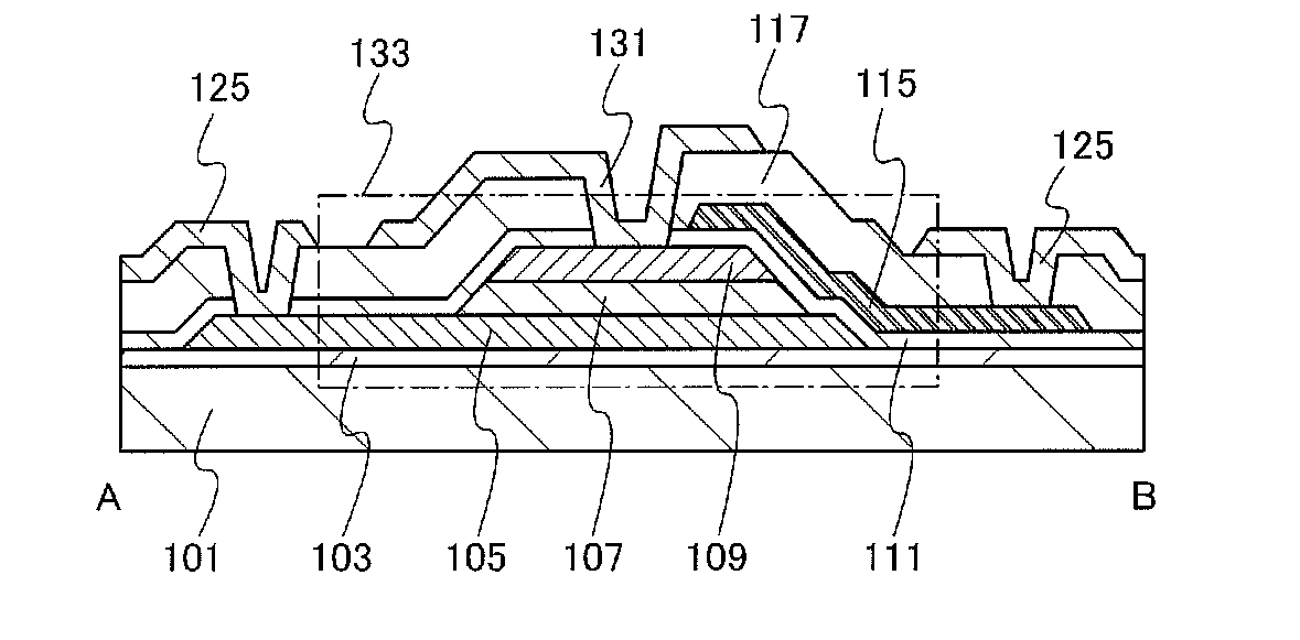
[0048]In this embodiment, a non-linear element which uses a vertical transistor including an oxide semiconductor according to an embodiment of the present invention will be described with reference to FIGS. 1A and 1B, FIGS. 2A and 2B, FIGS. 3A and 3B, FIGS. 4A to 4C, FIGS. 5A and 5B, and FIGS. 6A to 6D. An n-type oxide semiconductor is used here. The non-linear element described in this embodiment is obtained in such a manner that a gate electrode is connected to one of a source electrode and a drain electrode in the transistor, and the transistor is made to function as a diode.

[0049]In general, a diode has two terminals, i.e., an anode and a cathode. When a potential of the anode is higher than a potential of the cathode, the diode is in a state in which current flows, that is, a conduction state. On the other hand, when the potential of the anode is lower than the potential of the cathode, the diode is in a state in which current scarcely flows, that is, a non-conduction state (in...

embodiment 2

[0122]In this embodiment, an example of a non-linear element according to an embodiment of the present invention which has a structure different from that in Embodiment 1 will be described with reference to FIGS. 7A and 7B. The non-linear element described in this embodiment serves as a diode because a gate is connected to one of a source and a drain in a transistor.

[0123]In the diode illustrated in FIGS. 7A and 7B, a wiring 131 is connected to a first electrode 105 and a third electrode 113, and a wiring 132 is connected to a first electrode 106 and a third electrode 115. The first electrode 105 and the first electrode 106 are connected to a second electrode 109 through an oxide semiconductor layer 107. The second electrode 109 is connected to a wiring 129.

[0124]FIG. 7A is a top view of diode-connected transistors 141 and 143. FIG. 7B is a cross-sectional view along dashed-and-dotted line A-B in FIG. 7A.

[0125]As illustrated in FIG. 7B, the first electrode 105, the first electrode 1...

embodiment 3

[0134]In this embodiment, an example of a non-linear element according to an embodiment of the present invention which has a structure different from that in Embodiment 1 will be described with reference to FIGS. 9A and 9B. The non-linear element described in this embodiment functions as a diode because a gate is connected to one of a source and a drain in a transistor.

[0135]In the diode illustrated in FIGS. 9A and 9B, a wiring 131 is connected to a first electrode 105 and a third electrode 113. The first electrode 105 is connected to a second electrode 109 through an oxide semiconductor layer 107. The second electrode 109 is connected to a wiring 129.

[0136]FIG. 9A is a top view of a diode-connected transistor 145. FIG. 9B is a cross-sectional view along dashed-and-dotted line A-B in FIG. 9A.

[0137]As illustrated in FIG. 9B, the first electrode 105, the oxide semiconductor layer 107, and the second electrode 109 are stacked over an insulating layer 103 formed over a substrate 101. A ...


PUM


Abstract

A non-linear element (such as a diode) which includes an oxide semiconductor and has a favorable rectification property is provided. In a transistor including an oxide semiconductor in which the hydrogen concentration is 5×10¹⁹/cm3 or lower, a work function φms of a source electrode in contact with the oxide semiconductor, a work function φmd of a drain electrode in contact with the oxide semiconductor, and electron affinity χ of the oxide semiconductor satisfy φms≦χ<φmd, and an area of contact between the drain electrode and the oxide semiconductor is larger than an area of contact between the source electrode and the oxide semiconductor. By electrically connecting a gate electrode and the drain electrode in the transistor, a non-linear element having a favorable rectification property can be achieved.

Description

TECHNICAL FIELD[0001]An embodiment of the present invention relates to a non-linear element (e.g., a diode) including an oxide semiconductor and a semiconductor device such as a display device including the non-linear element. Further, an embodiment of the present invention relates to an electronic device including the semiconductor device.BACKGROUND ART[0002]Among semiconductor devices, diodes are required to have high withstand voltage, small reverse saturation current, and the like. Silicon carbide (SiC) used as a semiconductor material has a width of a forbidden band of 3 eV or more, excellent controllability of electric conductivity at high temperature, and a dielectric breakdown electric field that is about an order of magnitude higher than that of silicon. Therefore, silicon carbide is expected to be applied to a diode in which reverse saturation current is small and withstand voltage is high. For example, a Schottky barrier diode in which silicon carbide is used and reverse ...

Claims


Application Information

Patent Timeline
IPC IPC(8): H01L29/786
CPCH01L27/1225H01L29/78606H01L29/78642H01L29/78696H01L29/78648H01L29/7869H01L29/78645
Inventor KAWAE, DAISUKEUOCHI, HIDEKIYAMAZAKI, SHUNPEI
Owner SEMICON ENERGY LAB CO LTD
Why Eureka
Try Eureka