Supporting substrate for preparing semiconductor light-emitting device and semiconductor light-emitting device using supporting substrates

a technology for supporting substrates and semiconductor light-emitting devices, which is applied in semiconductor/solid-state device manufacturing, semiconductor devices, electrical devices, etc., can solve the problems of reducing the reliability of devices, unable to apply a large current to leds, and a lot of constraints in packaging processes, so as to improve the production yield of led chips, reduce the risk of micro-cracks or breaks, and reduce the effect of micro-cracks

Inactive Publication Date: 2011-06-02
LG INNOTEK CO LTD
View PDF10 Cites 50 Cited by
  • Summary
  • Abstract
  • Description
  • Claims
  • Application Information

AI Technical Summary

Benefits of technology

[0044]As mentioned above, the present invention provides an easy method for manufacturing a vertical-structured light-emitting device by arranging the first and second ohmic contact electrodes on the upper part and the lower part of the Group III-V nitride-based semiconductor single crystal multi-layered light-emitting structure, respectively, to improve the production yield of LED chips and separating the sapphire substrate for efficient heat dissipation and prevention of static electricity. Further, the present invention minimizes micro-crack or breaking in the Group III-V nitride-based semiconductor and separates the Group III-V nitride-based semiconductor thin film into wafer bonding materials by performing wafer bonding not to have any wafer warpage in the supporting substrate for preparing a semiconductor light-emitting device before separating the sapphire substrate by using the laser lift-off process, thereby reducing the stress applied to the Group III-V nitride-based semiconductor layers during the separation of the sapphire substrate from the Group III-V nitride-based semiconductor multi-layered light-emitting structure by using the laser life-off process.
[0045]In addition, when the Group III-V nitride-based semiconductor multi-layered light-emitting structure is formed on the upper part of the supporting substrate for preparing a semiconductor light-emitting device, since any post-processing such as annealing, passivation, etc. can be performed in the present invention, it is possible to provide a highly reliable light-emitting device that causes no thermal or mechanical damage. In addition, when the high reliability light-emitting device formed on the upper part of the supporting substrate for preparing a semiconductor light-emitting device is performed for a unified chip process, the method of the present invention allows a high production yield and productivity that could not be achieved in the wafer bonding process with conventional supporting substrates, since wet etching can be used in the present invention rather than in the conventional mechanical and laser processes.
[0046]The supporting substrate for preparing a semiconductor light-emitting device allows not only the manufacturing of a high quality nitride-based semiconductor single crystal multi-layered thin film by employing wafer bonding but also any kind of post-processing after separating the sapphire substrate so that it is suitable for manufacturing high performance vertical-structured Group III-V nitride-based light-emitting devices.
[0047]Further, the present invention allows the manufacturing of a single-chip-type semiconductor light-emitting device by using a sacrificial layer formed on the supporting substrate for preparing a semiconductor light-emitting device without any mechanical processing such as sawing, laser scribing, etc. of the light-emitting device formed on the “supporting substrate for preparing a semiconductor light-emitting device” wafer of the present invention.

Problems solved by technology

However, since the sapphire initial substrate has poor thermal conductivity, it cannot apply a large current to LEDs.
Since the sapphire initial substrate is an electrical insulator and thereby is difficult to respond to static electricity flowed in from outside, it has a high possibility to cause failure due to the static electricity.
Such drawbacks not only reduce reliability of devices but also cause a lot of constraints in packaging processes.
Since an LED chip area should be higher than a certain size, there is limit to reducing the LED chip area, restricting the improvement of LED chip production.
In addition to these disadvantages of the MESA-structured LEDs grown on the upper part of the sapphire substrate as an initial substrate, it is difficult to release a great amount of heat outward generated inevitably during the operation of the light-emitting device since the sapphire substrate has poor thermal conductivity.
Due to these reasons, there is a limitation in applying the MESA structure, to which the sapphire substrate is attached, to light-emitting devices used for a large area and a large capacity (that is, a large current) such as the light for large displays and general lighting.
However, because producing a high quality SiC substrate is not easy, it is more expensive than producing other single crystal substrates, making it difficult for mass production.
However, it has been reported in many documents that in the laser lift-off process of the Group III-V nitride-based semiconductor multi-layered light-emitting structure thin film, the semiconductor single crystal thin film is damaged and broken after being separated from the sapphire substrate due to a mechanical stress generated between the thick sapphire initial substrate and the Group III-V nitride-based semiconductor thin film because of the difference in the lattice constant and thermal expansion coefficient.
When the Group III-V nitride-based semiconductor multi-layered light-emitting structure thin film is damaged and broken, it causes a large leaky current, reduces the chip yield of light-emitting devices and reduces the overall performance of the light-emitting devices.
However, the supporting substrate 340, used for the vertical-structured light-emitting device (LED) as shown in (a) of FIG. 3, causes significant wafer warpage and fine micro-cracks inside the semiconductor multi-layered light-emitting structure when Si or another conductive supporting substrate wafer is bonded by wafer bonding because it has a significant difference in thermal expansion coefficient (TEC) against the sapphire substrate on which the semiconductor single crystal thin film is grown / laminated.
Such problems further cause processing difficulties and lower the performance of LED manufactured therefrom and the product yield.

Method used


Image

  • Supporting substrate for preparing semiconductor light-emitting device and semiconductor light-emitting device using supporting substrates
  • Supporting substrate for preparing semiconductor light-emitting device and semiconductor light-emitting device using supporting substrates
  • Supporting substrate for preparing semiconductor light-emitting device and semiconductor light-emitting device using supporting substrates

Examples


example 1

PREPARATION OF A SUPPORTING SUBSTRATE FOR PREPARING A SEMICONDUCTOR LIGHT-EMITTING DEVICE

Preparation Example 1

Preparation of a Supporting Substrate for Preparing a Semiconductor Light-Emitting Device

[0071]Hereinafter, the structure of a supporting substrate for preparing a semiconductor light-emitting device and its sequential manufacturing method according to an embodiment of the present invention will be described.

[0072]FIG. 4(a) is a sectional view illustrating a supporting substrate for preparing a semiconductor light-emitting device according to an embodiment of the invention.

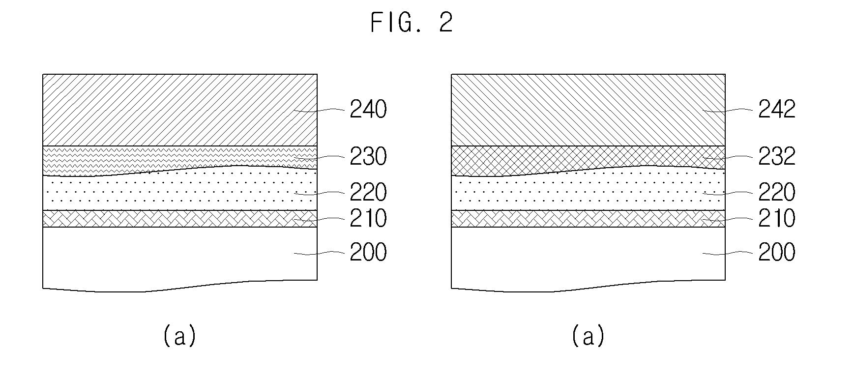
[0073]Referring to FIG. 4(a), a supporting substrate for preparing a semiconductor light-emitting device 40 includes a selected supporting substrate 400, a sacrificial layer 410, a heat-sink layer 420, and a bonding layer 430.

[0074]A method for manufacturing the above-mentioned supporting substrate for preparing a semiconductor light-emitting device 40 includes: (a) preparing a selected supporting substrat...

example 2

PREPARATION OF A SEMICONDUCTOR LIGHT-EMITTING DEVICE USING A SUPPORTING SUBSTRATE FOR PREPARING A SEMICODUCTOR LIGHT-EMITTING DEVICE

preparation example 1

Preparation of a Semiconductor Light-Emitting Device

[0104]Hereinafter, the structure of a semiconductor light-emitting device using a supporting substrate for preparing a semiconductor light-emitting device and its manufacturing method according to an embodiment of the present invention will be described.

[0105]FIG. 7 is a sectional view illustrating a semiconductor light-emitting device manufactured by using the supporting substrate for preparing a semiconductor light-emitting device according to Example 1 of the present invention. A semiconductor light-emitting device 70 in FIG. 7 is a light-emitting device manufactured by using a supporting substrate for preparing a semiconductor light-emitting device including a heat-sink layer 780 having the thin thickness of 80 μm or less.

[0106]The semiconductor light-emitting device 70 is formed by laminating a first ohmic contact electrode 780, a buffering layer 710, an n-type semiconductor cladding layer 720, a light-emitting active layer 73...


PUM


Abstract

The present invention is related to a supporting substrate for preparing a semiconductor light-emitting device employing a multi-layered light-emitting structure thin-film and a method for preparing a semiconductor light-emitting device employing the supporting substrate for preparing a semiconductor light-emitting device. The supporting substrate for preparing a semiconductor light-emitting device is formed by successively laminating a sacrificial layer, a heat-sink layer and a bonding layer on a selected supporting substrate. A method for preparing a semiconductor light-emitting device employing the supporting substrate for preparing a semiconductor light-emitting device includes: preparing a first wafer in which a semiconductor multi-layered light-emitting structure is laminated / grown on an upper part of an initial substrate; preparing a second wafer which is a supporting substrate for preparing a semiconductor light-emitting device; bonding the second wafer on an upper part of the first wafer; separating the initial substrate of the first wafer from a result of the bonding; performing passivation after forming a first ohmic contact electrode on an upper part of the first wafer from which the initial substrate is separated; and preparing a single-chip by severing a result of the passivation.

Description

TECHNICAL FIELD[0001]The present invention relates to a supporting substrate for preparing a semiconductor light-emitting device using a multi-layered light-emitting structure thin film and a method for preparing a semiconductor light-emitting device using the supporting substrate for preparing a semiconductor light-emitting device.[0002]More particularly, in a Group III-V nitride-based semiconductor light-emitting device vertically structured in the up and down ohmic contact electrode structure, it relates to a semiconductor light-emitting device which minimizes damage to a semiconductor single crystal multi-layered light-emitting structure thin film, thereby improving the overall performance, by bonding a multi-layered light-emitting structure thin film formed on an initial substrate (e.g., Al2O3 , SiC, Si, GaAs, GaP) to grow the Group III-V nitride-based semiconductor and a supporting substrate for preparing a semiconductor light-emitting device through wafer bonding and then sep...

Claims


Application Information

Patent Timeline
Patent Type & Authority Applications(United States)
IPC IPC(8): H01L33/02H01L33/00H01L33/44H01L33/64
CPCH01L33/0079H01L33/0095H01L33/44H01L33/641H01L33/005H01L33/64H01L33/0075H01L33/40H01L33/42H01L33/60H01L33/48H01L21/6835H01L33/007H01L2221/68318H01L33/642H01L33/0093
Inventor SEONG, TAE YEON
Owner LG INNOTEK CO LTD
Why Eureka
Try Eureka