Method of growing a thin film, a method of forming a structure and a device

a thin film and structure technology, applied in the direction of sustainable manufacturing/processing, semiconductor/solid-state device details, instruments, etc., can solve the problems of not meeting the requirements of any of these methods, unable to achieve one preferred and well-controlled growth direction, and unable to achieve the desired device performance. achieve the effect of improving the quality accelerating the growth rate of the thin film, and controlling the rough surface of the final top surfa

Inactive Publication Date: 2011-06-16
SHARP KK
View PDF4 Cites 24 Cited by
  • Summary
  • Abstract
  • Description
  • Claims
  • Application Information

AI Technical Summary

Benefits of technology

[0101]Through the regularity and pitch of the nanostructures as well as their height compared to the final film thickness, the surface roughness of the final top surface can be controlled. For some applications, it may be required to planarise the upper surface of the film once it has been deposited, using suitable polishing techniques, for example to provide a planar surface for deposition of further layers of a device structure. In other cases a rough surface can be desirable to couple more light into the active region of a photovoltaic device. The surface roughness can be tailored to particular requirements by optimising the regularity and pitch of the nanostructures as well as their height compared to the final film thickness.
[0102]A further embodiment of the invention is that the structures may act as templates for the growth of high quality materials. It is for example well known that semiconductor nanowires can be grown without defects or with a low defect density on highly mismatched substrates. Also, it is known from the scientific literature that nanowires can be used as seeds to grow epitaxially concentric layers (shells) around them which can be done without depositing material on non-crystalline surfaces (so-called selective epitaxial growth). The shell may consist of a material different to the nanowire This growth on a crystalline substrate can be coherent (defect free) at the nanowire-shell interface even if there is a lattice mismatch between the material of the shell and the material of the nanowire. This is due to the fact that the strain can relax along the outer surface of the nanowire.
[0103]In a further embodiment, the embedded nano structures within the thin film are removed. This can be achieved, for example, by removing the top parts of the thin film structure after the enhanced thin film growth process ((a) of FIG. 15) via suitable techniques (e.g. anisotropic etching, polishing etc) to leave the nano structures exposed ((b) of FIG. 15). These nano structures are then removed by suitable methods (e.g. etching) ((c) of FIG. 15). Material is then deposited to fill the empty volume left by the nano structures ((d) of FIG. 15). This embodiment will offer the opportunity not only to accelerate the thin film growth rate, but also to grow a better quality thin film (i.e. fewer defects) without containing materials that are not a part of thin film (i.e. the original nano structures).

Problems solved by technology

Growth conditions and substrates can be chosen such that the growth direction of the nanowire or nanorod is essentially vertical to the substrate surface, although on non-crystalline substrates achieving one preferred and well controlled growth direction remains an unsolved challenge.
One reason why this kind of nanowire growth is difficult to use in an industrial process lies in the need of a catalyst, which tends to leave metal impurities in the wire which are usually detrimental to the desired device performance.
However, none of these methods fulfils all of the following requirements simultaneously:1) To provide the low level of impurities which is necessary to obtain high quality, high performing semiconductor devices like CMOS transistors and inorganic solar cells;2) To grow at a rate exceeding the rate expected from planar thin film growth on a planar substrate at the same deposition rate;3) To make more efficient use of the process gases compared to horizontal thin film growth at the same deposition rate;4) To introduce a controlled degree of roughness of the top surface;5) To offer a method forming an interlaced device without requiring any specific nanowire growth steps;6) To offer precise control to configure the interlaced device structure.
To achieve this, merging of adjacent nanowires had to be minimised as much as possible, leaving a large amount of the volume between the nanowires void.
Furthermore, the method disclosed does not enable the fabrication of a template comprising an array of pores with well defined dimensions (e.g. variations of pitch and diameter of less than 10%).
Also, the use of metal-based templates potentially restricts the time-temperature budget of subsequent process steps due to the risk of metal contamination.
This may not impose concerns regarding the fabrication of organic solar cells, but its compatibility with the process steps required to fabricate inorganic solar cells (e.g. Si-based solar cells) is questionable.
Hence, the dimensions disclosed (e.g. a pitch of the pores below 500 nm) may too small to accommodate all of the material required to form an efficient inorganic solar cell—especially if additional layers such as diffusion barriers, electrical contacts and anti-reflection coatings need to be accommodated.

Method used


Image

  • Method of growing a thin film, a method of forming a structure and a device
  • Method of growing a thin film, a method of forming a structure and a device
  • Method of growing a thin film, a method of forming a structure and a device

Examples


Embodiment Construction

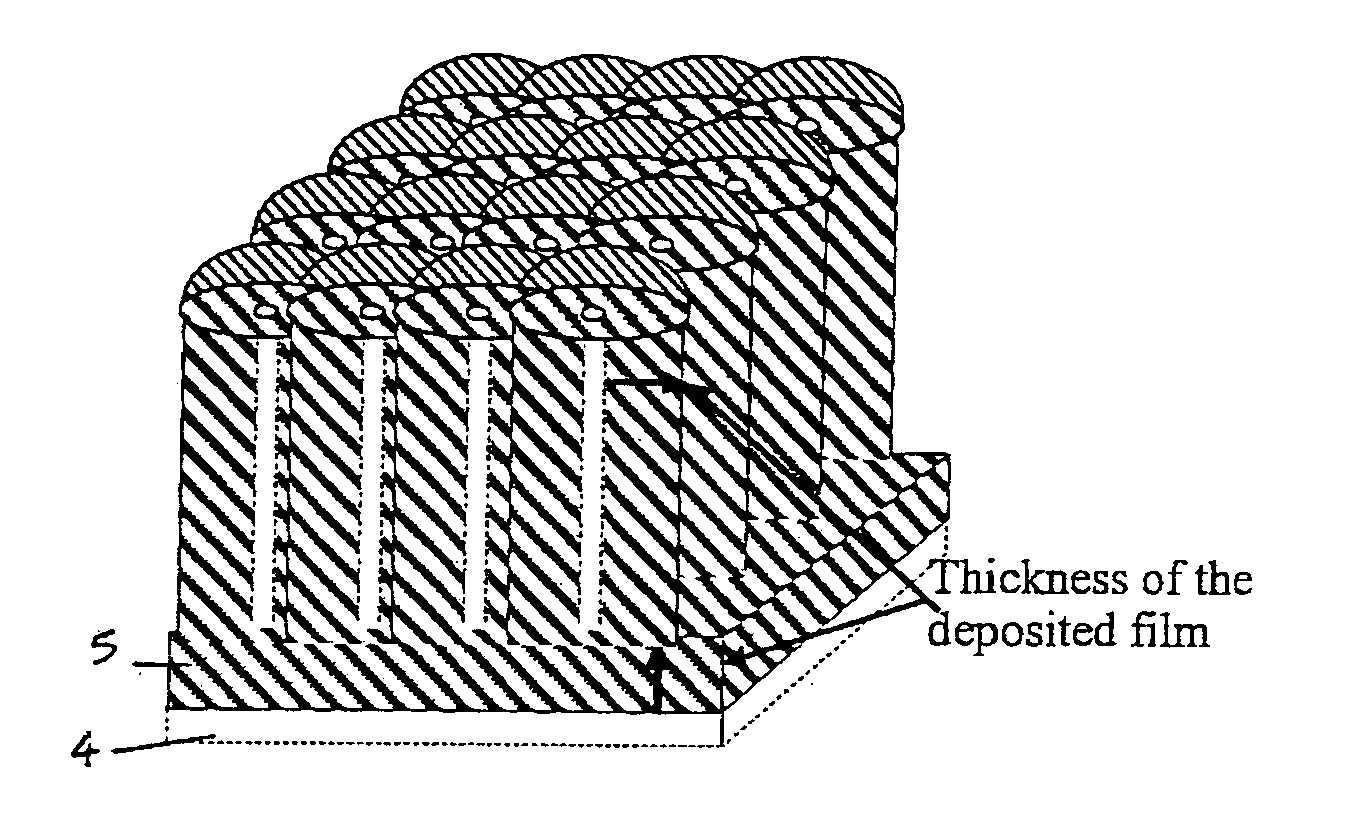
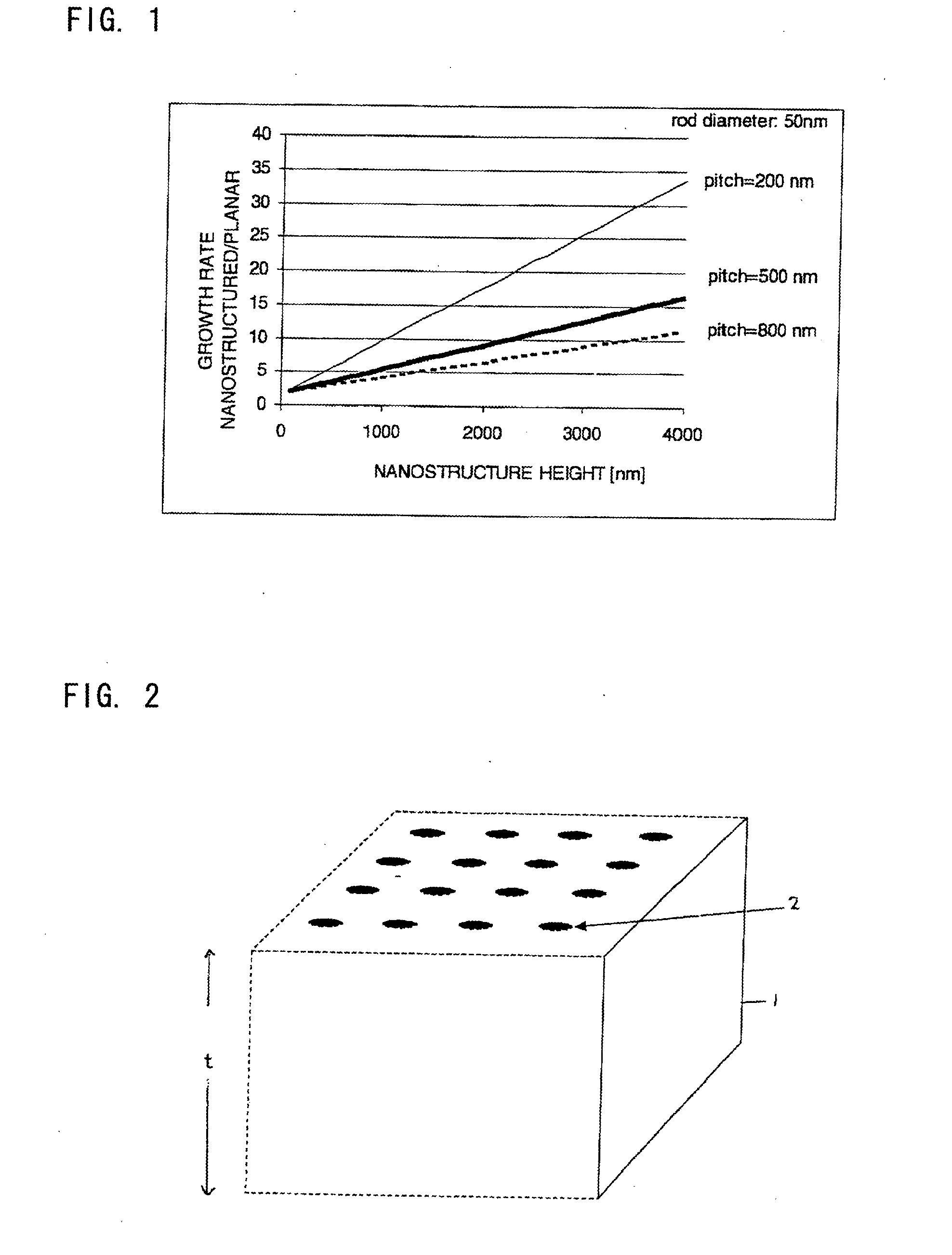
[0122]In a preferred embodiment according to FIG. 2a substrate 1 of thickness t with an appropriately patterned etch mask 2 is provided. The patterned etch mask 2 can be defined by lithographic means.

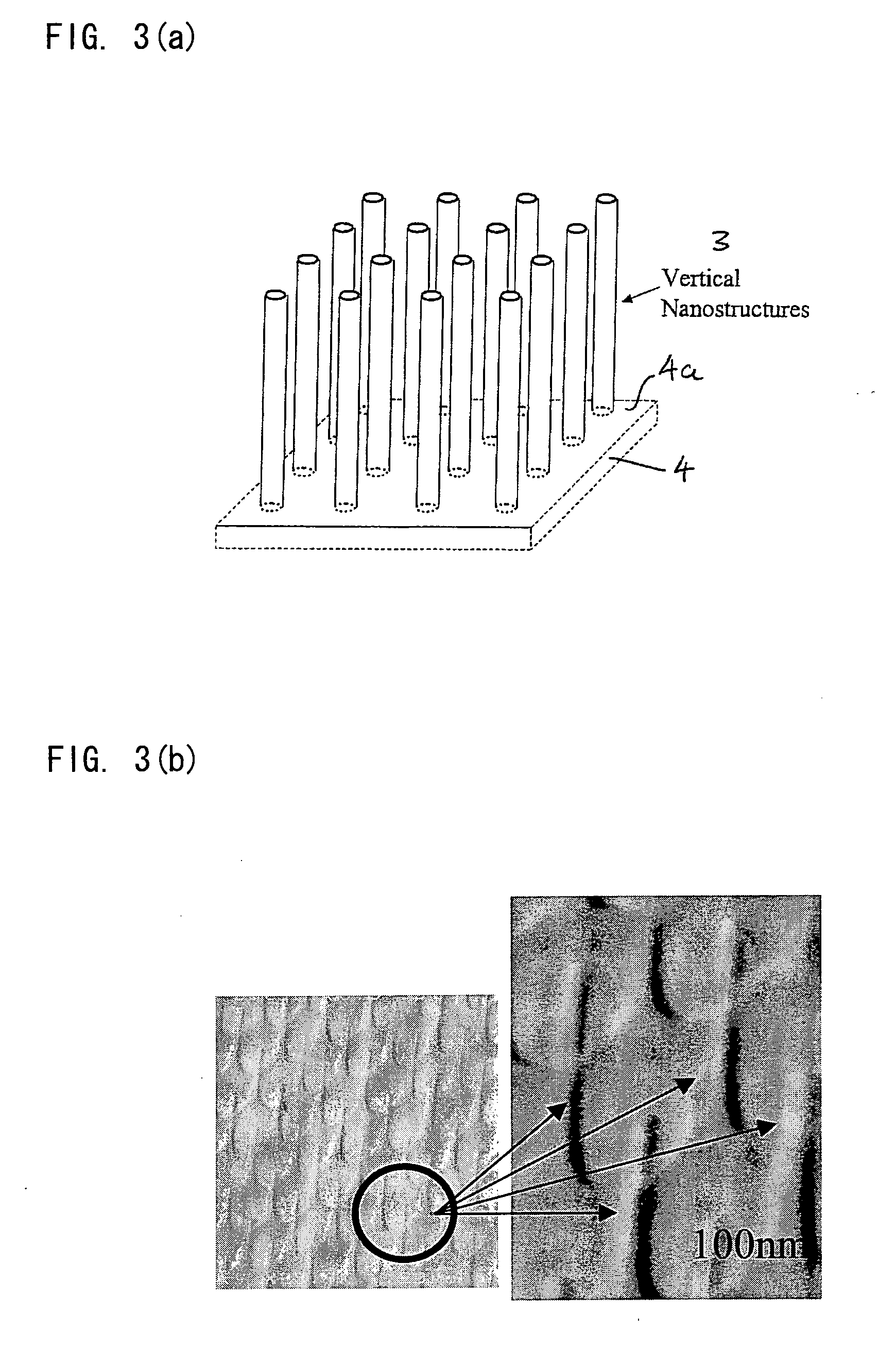
[0123]Subsequently a substantially anisotropic, subtractive process is used to create the nanostructures 3 on substrate 4 (FIG. 3(a)). Optionally, the nanostructures 3 are formed so that they have a uniform or substantially uniform pitch and / or have a uniform or substantially uniform length. Optionally, the nanostructures 3 are formed so that the structures are identical or substantially identical to one another.

[0124]If desired, the nanostructures can be thinned further using an isotropic etch process. This may also change the shape of the structures in a preferred way (e.g. by providing a taper).

[0125]The etch mask 2 may be removed if desired, once the / all etching steps are complete.

[0126]The etch mask 2 may for example comprise a metal (e.g. Al, Au, W) or a nitride (e.g. Si3N4).

[0127...


PUM

PropertyMeasurementUnit
angleaaaaaaaaaa
angleaaaaaaaaaa
angleaaaaaaaaaa

Abstract

A method of growing a thin film comprises growing a thin film by conformally forming at least one layer over a substrate having structures extending from a surface of the substrate, whereby the or each layer is formed over the surface of the substrate and over the structures extending from the surface. The thickness of the conformal layer, or the sum of the thicknesses of the conformal layers, is at least half the average spacing of the structures, and; at least one of the height of the structures, the average spacing of the structures and the size of the smallest dimension of the structures is set so as to provide an enhanced growth rate for the or each conformal layer (compared to the growth rate over a planar substrate).

Description

TECHNICAL FIELD[0001]The present invention relates to the growth of a thin film on a substrate. In particular it relates to enhancing the growth rate of a thin film (compared to growth over a planar substrate) by conformal deposition on a structured substrate.BACKGROUND ART[0002]The growth of thin films is a core process in the production of many electronic and optoelectronic devices. It is also often the most costly and time consuming step and any increase in the efficiency of thin film deposition would almost certainly lead to a reduction of the production costs.[0003]Thin films are deposited onto a substrate material which carries them. Substrates can be made up of virtually any solid material. One of the main criteria for a substrate is that it has to withstand the process conditions during the thin film deposition and subsequent processing, especially with respect to the temperature.[0004]Thin films can be deposited in a variety of ways including chemical vapour deposition (CVD...

Claims


Application Information

Patent Timeline
Patent Type & Authority Applications(United States)
IPC IPC(8): H01L31/04B05D1/36B05D5/12C23C16/00B32B3/10H01L21/20H01L29/40B82Y99/00
CPCB82Y10/00H01L21/0237H01L21/0243H01L21/02521H01L21/02658H01L31/0232Y10T428/24364H01L31/18H01L2924/0002H01L31/0352Y10T428/24355H01L2924/00H01L31/03529H01L31/1804H01L31/0543Y02E10/52Y02E10/547Y02E10/548Y02P70/50H01L21/2003
Inventor LANG, CHRISTIANHUANG, YING JUN JAMESALTEBAEUMER, THOMAS HEINZ-HELMUTDAY, STEPHENHEFFERNAN, JONATHAN
Owner SHARP KK
Why Eureka
Try Eureka