

Ion beam device
a technology of ion beam and ion beam, which is applied in the direction of beam deviation/focusing, instruments, heat measurement, etc., can solve the problems of ionized gas supplied to the gas ionization chamber thus inevitably leakage, the resolution of the sample observation degrades, and no prior art measures have been taken for the leakage of ionized gas from the gas ionization chamber. , to achieve the effect of enhancing the focusing performance of the i
- Summary
- Abstract
- Description
- Claims
- Application Information
AI Technical Summary
Benefits of technology
Problems solved by technology
Method used
Image

Examples
Embodiment Construction
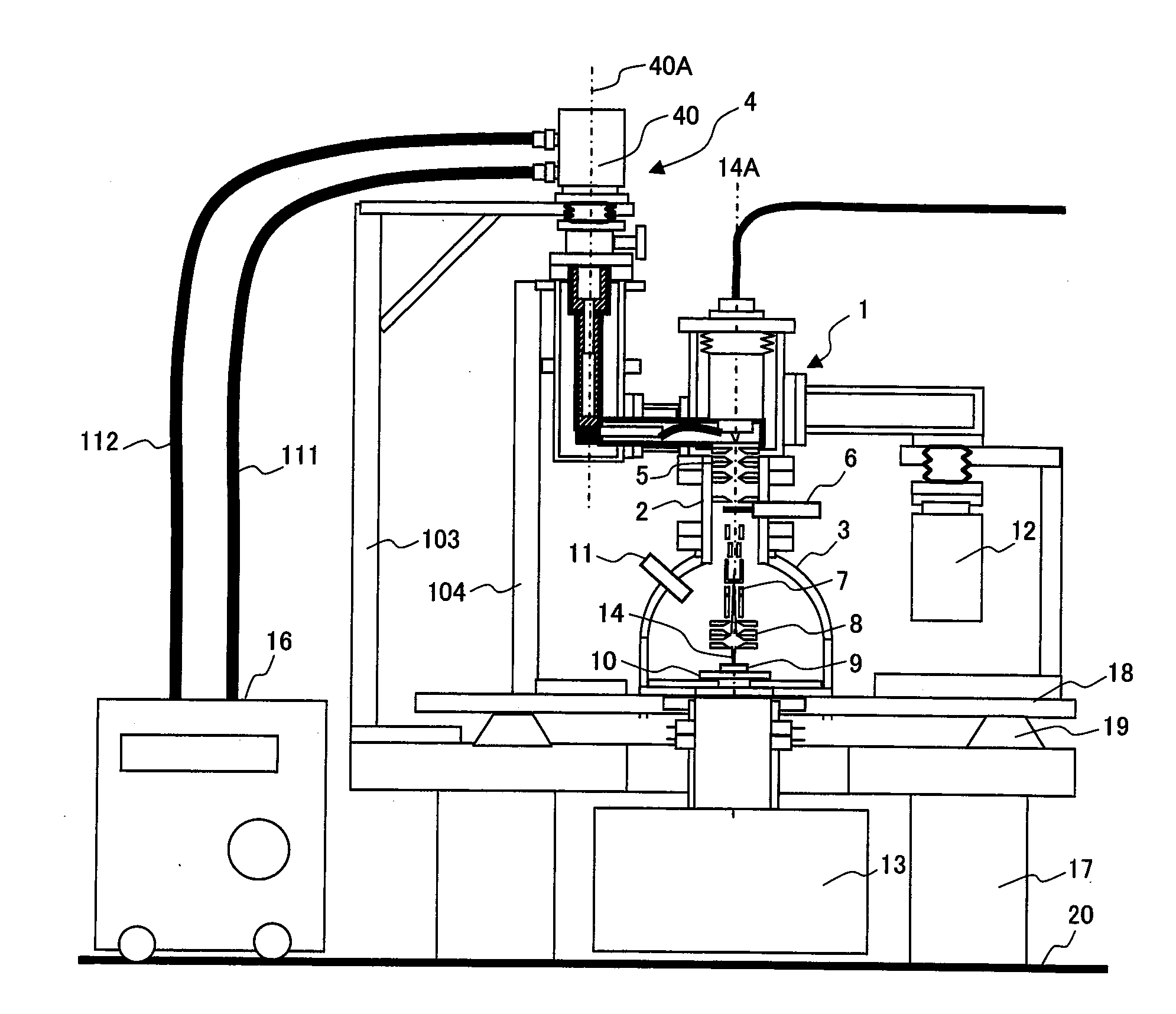
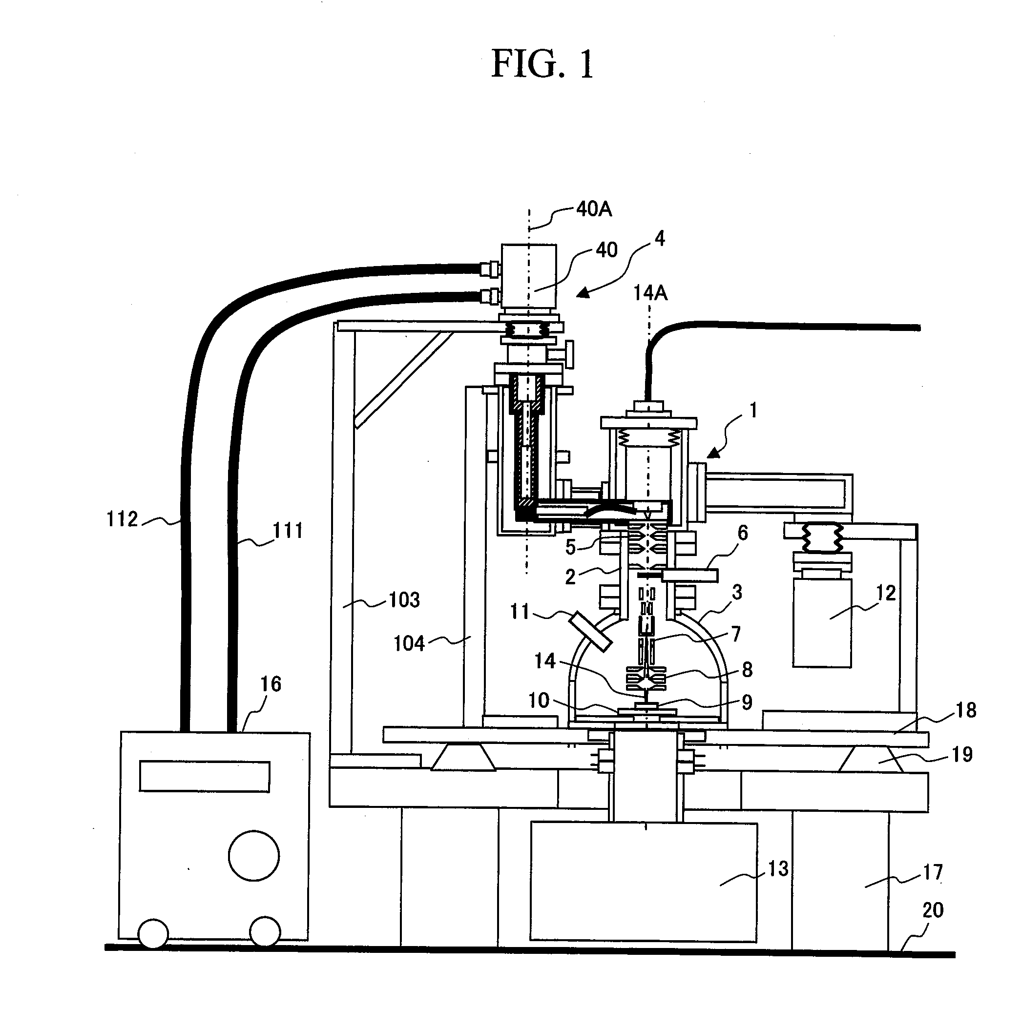
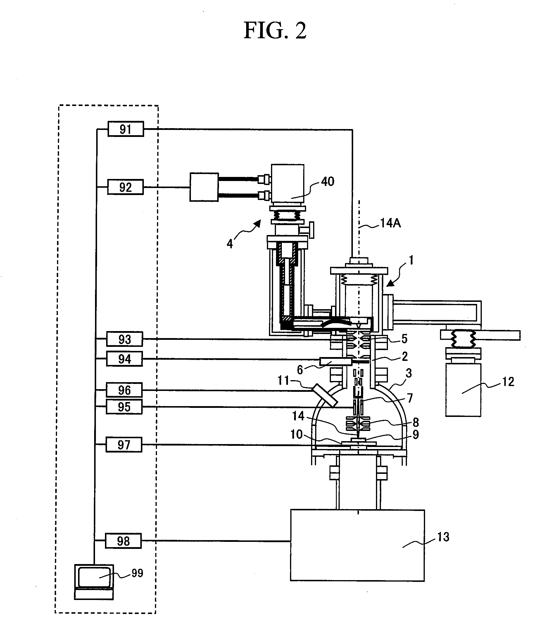
[0164]An example of an ion beam device according to the present invention will be described with reference to FIG. 1. A first example of a scanning ion microscope device will be hereinafter described as the ion beam device. The scanning ion microscope of the present example includes a gas field ion source 1, a column 2, a sample chamber 3, and a cooling mechanism 4. The inside of the column 2 and the sample chamber 3 is held in vacuum, and an ion beam irradiation system is arranged therein. The ion beam irradiation system includes an electrostatic condenser lens 5, a beam limiting aperture 6, a beam scanning electrode 7, and an electrostatic objective lens 8. A sample stage 10 for mounting a sample 9 and a secondary particle detector 11 are arranged in the sample chamber 3. An ion beam 14 from the gas field ion source 1 is irradiated onto the sample 9 through the ion beam irradiation system. The secondary particle beam from the sample 9 is detected by the secondary particle detector...
PUM
 Abstract
Description
Claims
Application Information