Photoelectric conversion device manufacturing method, photoelectric conversion device, and photoelectric conversion device manufacturing system

a technology of photoelectric conversion device and manufacturing method, which is applied in the manufacture of final products, sustainable manufacturing/processing, coatings, etc., can solve the problems of large amount of energy spent, high manufacturing cost, and significant cost increase, and achieve the capability of a thin-film photoelectric conversion device and suppress an indistinct junction. , the effect of excellent impurity profil

Inactive Publication Date: 2011-06-30
ULVAC INC
View PDF5 Cites 1 Cited by
  • Summary
  • Abstract
  • Description
  • Claims
  • Application Information

AI Technical Summary

Benefits of technology

According to the method of the present invention for manufacturing a photoelectric conversion device, since the plasma-CVD reaction chamber, in which the first p-type semiconductor layer, the first i-type semiconductor layer, the first n-type semiconductor layer of the first-photoelectric conversion unit, or the second i-type semiconductor layer of the second-photoelectric conversion unit is formed, is different from the plasma-CVD reaction chamber in which the second p-type semiconductor layer of the second-photoelectric conversion unit is formed, it is possible to suppress an indistinct junction caused by impurities in the second p-type semiconductor layer constituting the second-photoelectric conversion unit being diffused in the second i-type semiconductor layer or remaining impurities being doped into the second p-type semiconductor layer and the second n-type semiconductor layer.
Also, due to the p-type semiconductor layer of the second-photoelectric conversion unit being exposed to an air atmosphere, a crystal core is generated which is caused by OH being adhered to the top face of the p-type semiconductor layer or part of the surface of the p-layer being oxidized, and the crystallization rate of the i-type semiconductor layer of the second-photoelectric conversion unit composed of a crystalline-silicon-based thin film increases.
Additionally, since the photoelectric conversion device of the present invention is formed by the above-described photoelectric conversion device manufacturing method, an excellent impurity profile is obtained in the pin junction structure.
Because of this, it is possible to obtain an excellent capability of a thin-film photoelectric conversion device while an indistinct junction is not generated.
Furthermore, according to the photoelectric conversion device of the present invention manufacturing system, the first p-type semiconductor layer, the first i-type semiconductor layer, the first n-type semiconductor layer of the first-photoelectric conversion unit, and the second p-type semiconductor layer of the second-photoelectric conversion unit are formed in the first-film-formation apparatus. Additionally, the second i-type semiconductor layer and the second n-type semiconductor layer of the second-photoelectric conversion unit are formed in the second-film-formation apparatus. For this reason, it is possible to suppress an indistinct junction caused by impurities in the second p-type semiconductor layer constituting the second-photoelectric conversion unit being diffused in the second i-type semiconductor layer or remaining impurities being doped into the second p-type semiconductor layer and the second n-type semiconductor layer.
Therefore, it is possible to manufacture a photoelectric conversion device having an excellent capability.

Problems solved by technology

However, in contrast, in the photoelectric conversion device in which the silicon single crystal is utilized, single crystal silicon ingot is sliced, a sliced silicon wafer is used in the solar cell; therefore, a large amount of energy is spent for manufacturing the ingot, and the manufacturing cost is high.
For example, at the moment, in a case of realizing a photoelectric conversion device having a large area which is placed outdoors or the like, when being manufactured by use of single crystal silicon, the cost considerably increases.
However, conversion efficiency of a photoelectric conversion device in which an amorphous-silicon thin film is utilized is lower than the conversion efficiency of a crystalline photoelectric conversion device in which single-crystalline silicon or polysilicon is utilized.
However, in the case where the p, i, and n-layers of the crystalline photoelectric conversion-layer are formed in the same reaction chamber, since the processing is performed in the same reaction chamber, there is a problem in that an indistinct junction caused by impurities in the p-layer being diffused in an i-layer or caused by remaining impurities being doped into a p-layer and an n-layer is generated.

Method used


Image

  • Photoelectric conversion device manufacturing method, photoelectric conversion device, and photoelectric conversion device manufacturing system
  • Photoelectric conversion device manufacturing method, photoelectric conversion device, and photoelectric conversion device manufacturing system
  • Photoelectric conversion device manufacturing method, photoelectric conversion device, and photoelectric conversion device manufacturing system

Examples


experimental examples

Next, according to the photoelectric conversion device manufactured by the photoelectric conversion device manufacturing method related to the present invention, experiments were performed as described below.

The photoelectric conversion device manufactured by each Experimental Example and the manufacturing condition therefor is as follows.

In all of Experimental Examples described below, the photoelectric conversion device was manufactured by use of a substrate having lengths of 1100 mm and 1400 mm

(1) In Experimental Example described below, the relationship between the length of time a p-layer of a second-photoelectric conversion unit being exposed to an air atmosphere and photoelectric conversion characteristics was evaluated.

experimental example 1

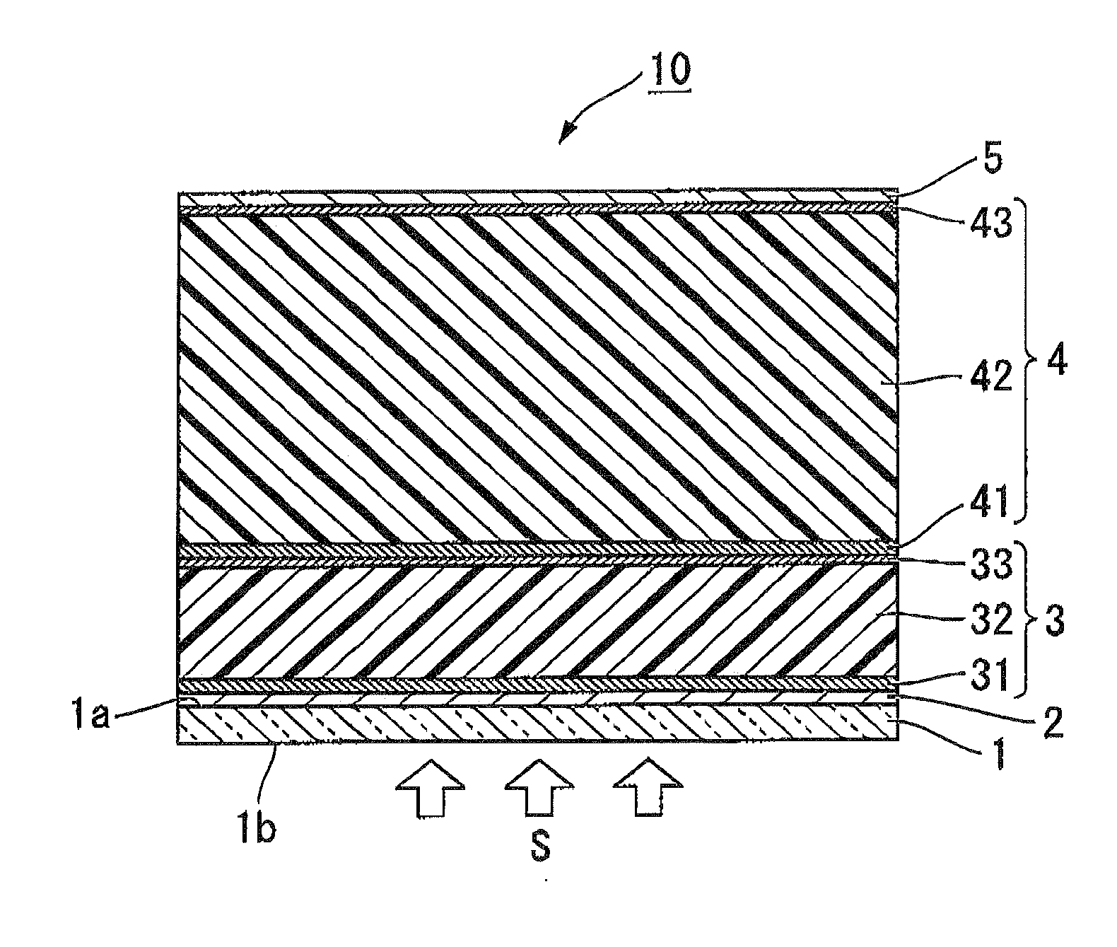
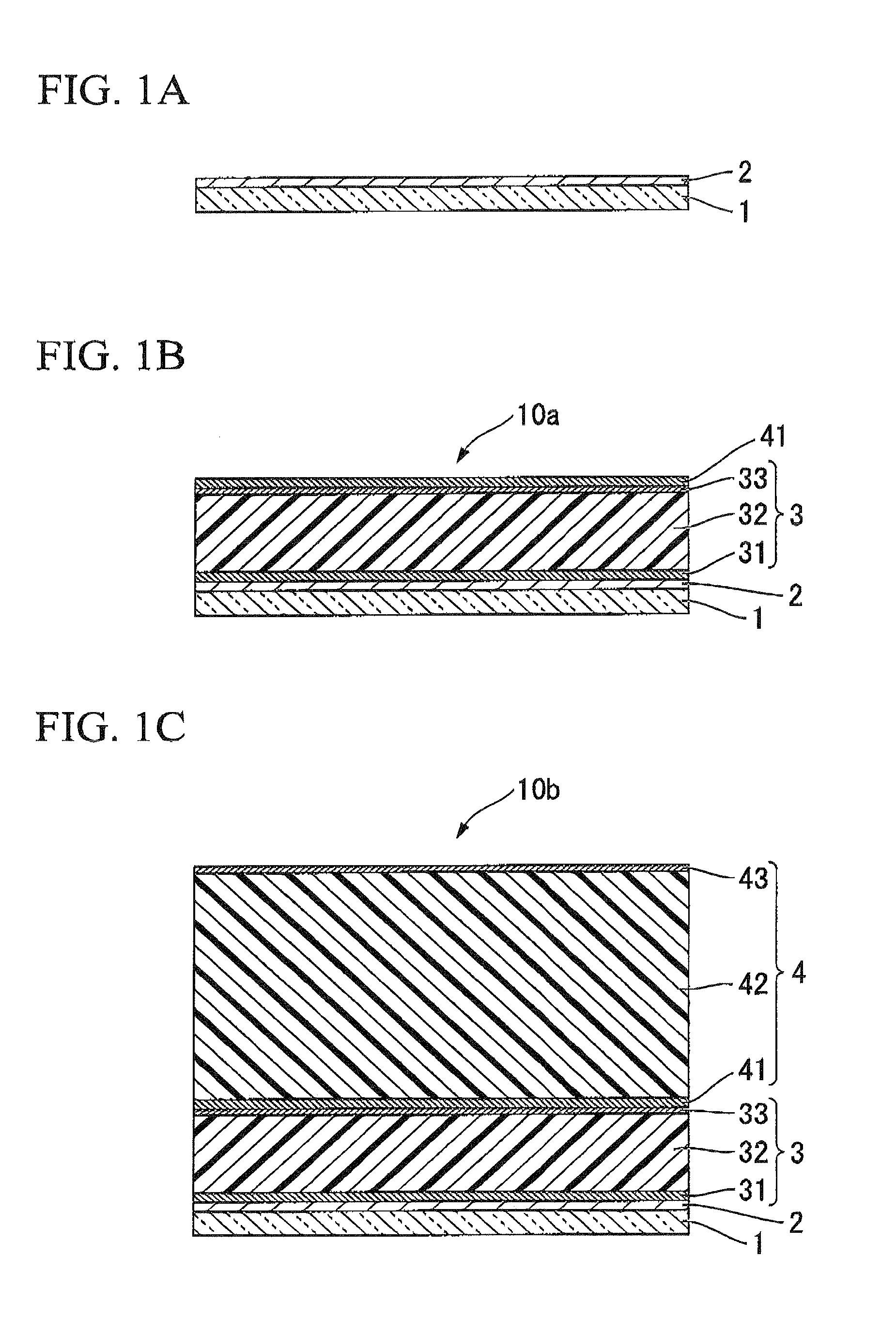
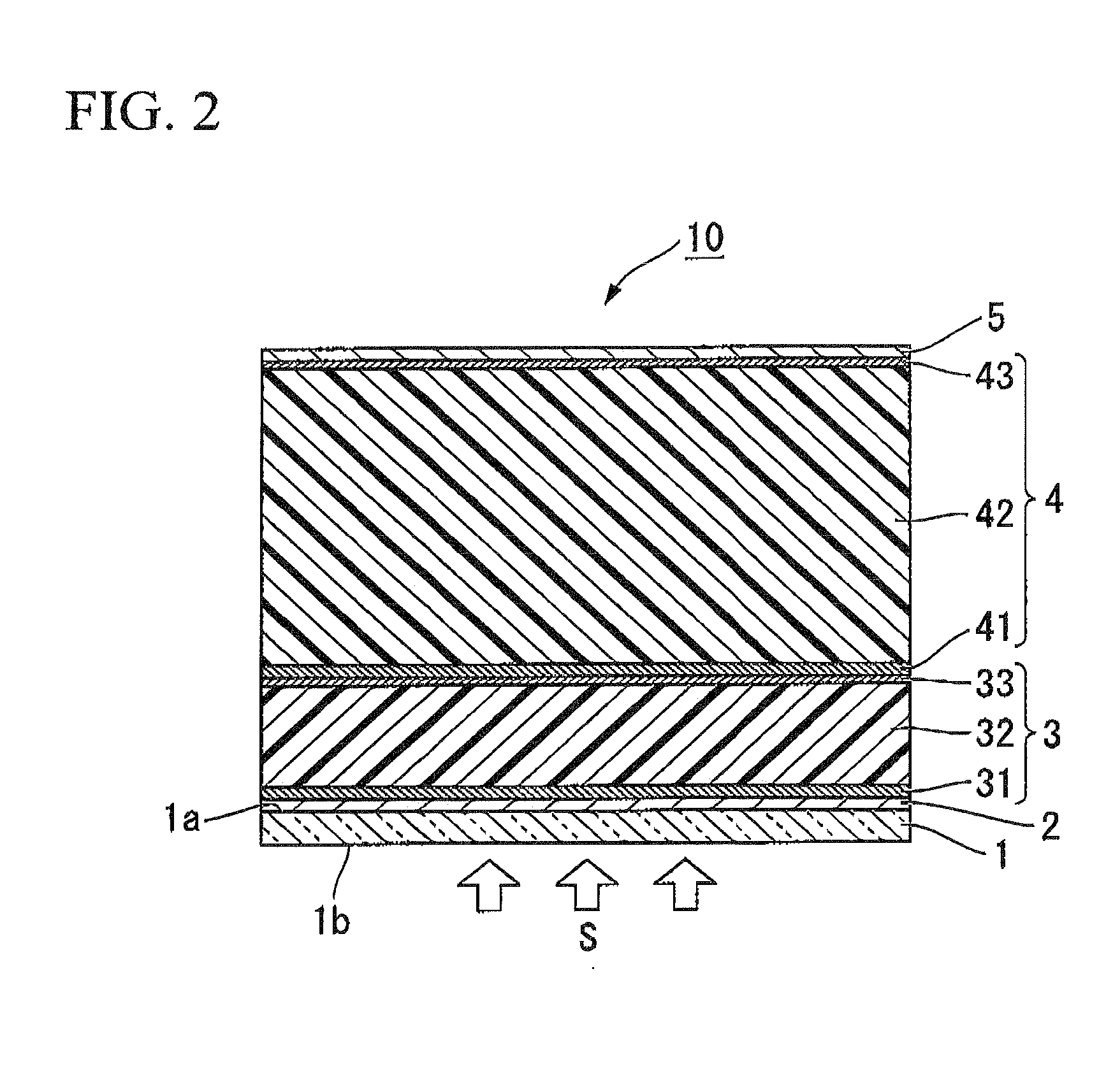
In Experimental Example 1, a p-layer and an i-layer which are composed of an amorphous silicon (a-Si) based thin film were formed on the substrate as a first-photoelectric conversion unit, an n-layer including microcrystalline silicon (μc-Si) was formed on the i-layer, and a p-layer that includes microcrystalline silicon (μc-Si) and constitutes a second-photoelectric conversion unit was formed.

The layers described above were continuously formed in a vacuum atmosphere, and reaction chambers in which the layers are formed were different from each other.

Thereafter, the p-layer of the second-photoelectric conversion unit was exposed to an air atmosphere, and the p-layer of the second-photoelectric conversion unit was subjected to a hydrogen radical plasma processing.

Subsequently, an i-layer and an n-layer, which constitute the second-photoelectric conversion unit and are composed of microcrystalline silicon (μc-Si), were formed.

In Experimental Example 1, the p-layer, the i-layer, and th...

experimental example 2

In this Experimental Example, in a manner similar to Experimental Example 1, after the p-layer, the i-layer, and the n-layer of the first-photoelectric conversion unit, and the p-layer of the second-photoelectric conversion unit were formed on the substrate, the p-layer of the second-photoelectric conversion unit was exposed to an air atmosphere for five minutes.

The p-layer was subjected to the hydrogen radical plasma processing for sixty seconds under conditions in which the substrate temperature was 170° C., the power source output was 500 W, the internal pressure of the reaction chamber was 400 Pa, and H2 which serves as a processing gas was 1000 sccm.

Subsequently, in a manner similar to Experimental Example 1, the i-layer and the n-layer of the second-photoelectric conversion unit were formed.


PUM

PropertyMeasurementUnit
frequencyaaaaaaaaaa
frequencyaaaaaaaaaa
frequencyaaaaaaaaaa

Abstract

A photoelectric conversion device manufacturing method, includes: continuously forming a first p-type semiconductor layer, a first i-type semiconductor layer, and a first n-type semiconductor layer, which constitute a first-photoelectric conversion unit, and a second p-type semiconductor layer which constitutes a second-photoelectric conversion unit composed of a crystalline-silicon-based thin film, in a reduced-pressure atmosphere; exposing the second p-type semiconductor layer to an air atmosphere; and forming a second i-type semiconductor layer and a second n-type semiconductor layer, which constitute the second-photoelectric conversion unit, on the second p-type semiconductor layer which was exposed to an air atmosphere.

Description

BACKGROUND OF THE INVENTION1. Field of the InventionThe present invention relates to a photoelectric conversion device manufacturing method, a photoelectric conversion device, and a photoelectric conversion device manufacturing system, particularly, technique of improving the performance of a tandem-type photoelectric conversion device which is configured so that two photoelectric conversion units are formed and stacked in layers therein.This application claims priority from Japanese Patent Application No. 2008-222818 filed on Aug. 29, 2008, the contents of which are incorporated herein by reference in their entirety.BACKGROUND ARTIn recent years, photoelectric conversion devices have been widely used for solar cells, photodetectors, or the like, in particular, in view of efficient use of energy, solar cells are more widely used than ever before.Specifically, a photoelectric conversion device in which single crystal silicon is utilized has a high level of energy conversion efficienc...

Claims


Application Information

Patent Timeline
Patent Type & Authority Applications(United States)
IPC IPC(8): H01L31/06H01L31/18H01L31/076H01L31/077
CPCC23C16/24H01L21/02532H01L21/02592H01L21/0262Y02E10/548H01L31/077H01L31/1824Y02E10/545H01L31/076Y02E10/547Y02P70/50H01L31/04H01L31/075H01L31/18
Inventor UCHIDA, HIROTAFUJINAGA, TETSUSHIUE, YOSHINOBUSAITO, KAZUYANAKAMURA, KYUZO
Owner ULVAC INC
Why Eureka
Try Eureka