
Semiconductor resistors formed at a lower height level in a semiconductor device comprising metal gates

a technology of resistors and semiconductors, applied in semiconductor devices, diodes, electrical apparatus, etc., can solve the problems of reduced threshold voltage, significant increase of leakage current, and high complexity of circuits, so as to avoid any negative influence of conductive materials on the overall electronic characteristics of resistive structures, reliably suppress the exposure of semiconductor materials in the resistive structure, and efficiently apply

Active Publication Date: 2011-06-30
GLOBALFOUNDRIES US INC
View PDF4 Cites 22 Cited by
  • Summary
  • Abstract
  • Description
  • Claims
  • Application Information

AI Technical Summary

Benefits of technology

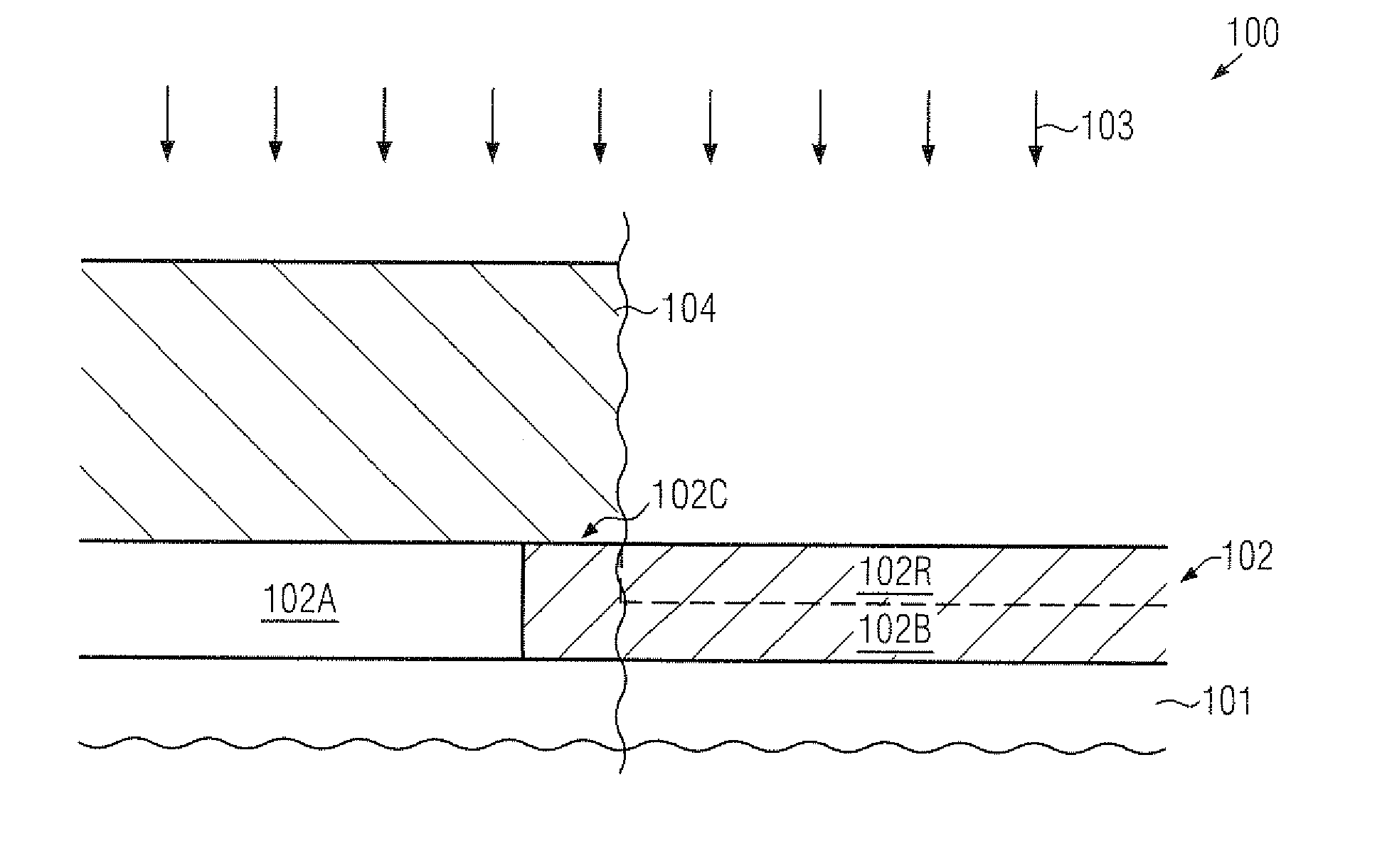
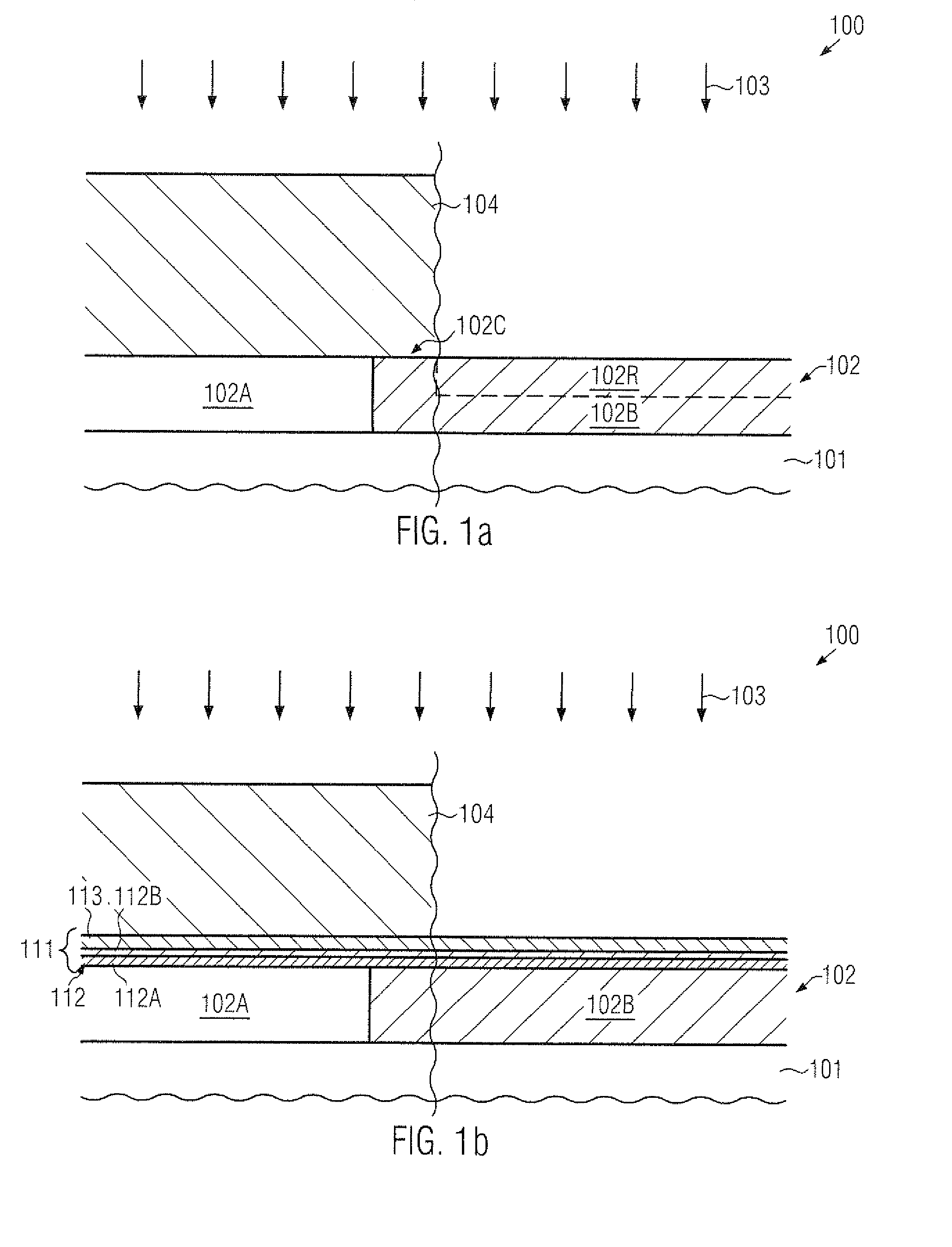
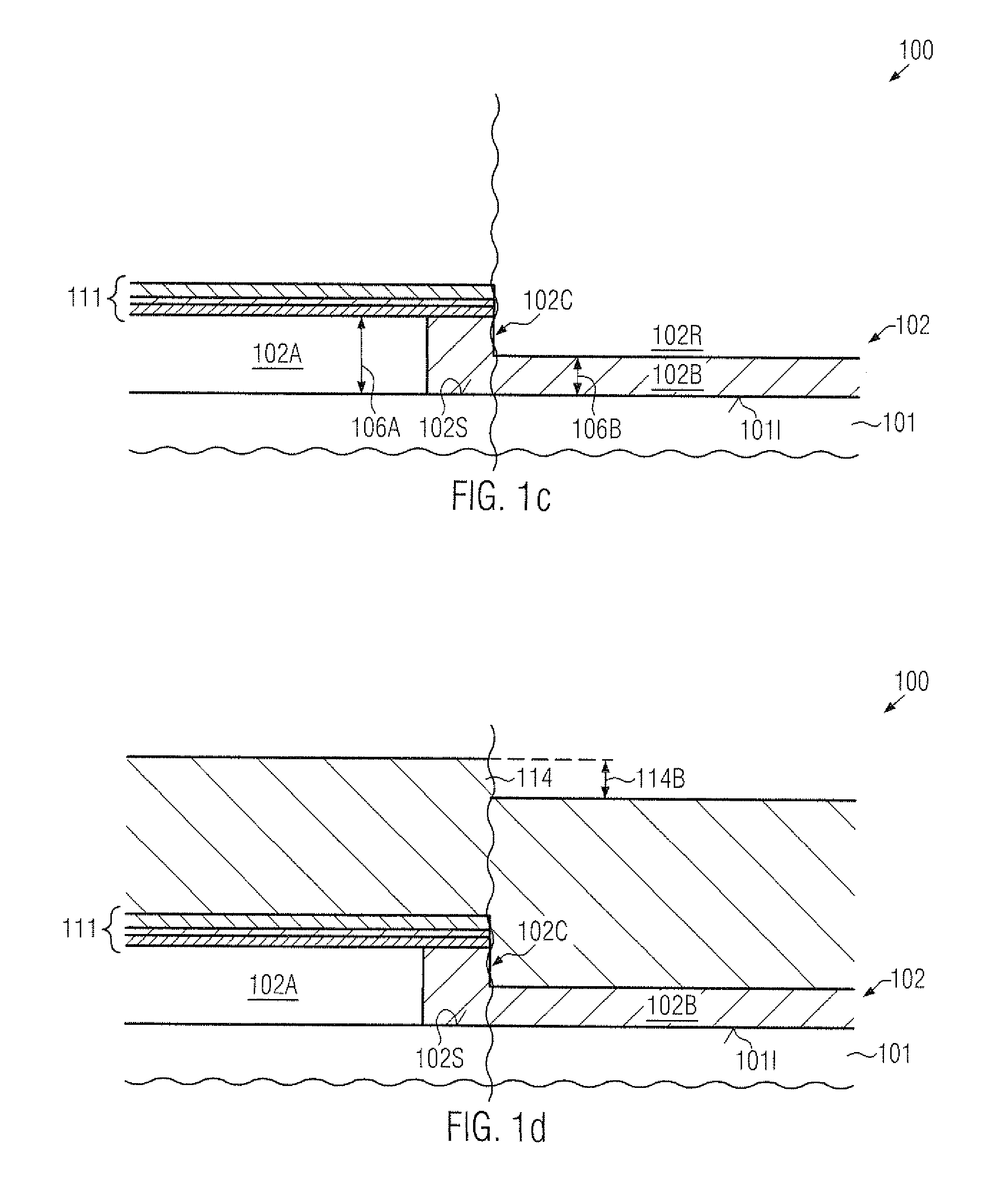
[0014]The present disclosure generally provides semiconductor devices and manufacturing techniques in which resistive structures or resistors may be formed on the basis of an appropriate semiconductor material, such as a polysilicon material, a silicon / germanium material and the like, while, at the same time, sophisticated high-k metal gate electrode structures may be provided on the basis of a replacement gate approach. To this end, the semiconductor material of the resistive structures may be reliably preserved upon replacing the semiconductor material of the replacement gate electrode structures by ensuring that, upon exposing the top surface of the semiconductor material in the gate electrode structures, an exposure of the semiconductor material in the resistive structure is reliably suppressed. For this purpose, in some illustrative aspects disclosed herein, an appropriate device topography may be provided such that the top surface of the semiconductor material in the resistive structure may be positioned at a height level that is less or lower than a height level of the top surface of the semiconductor material in the replacement gate electrode structure. Consequently, upon performing a material removal process, such as a polishing process, a certain amount of dielectric material may still be preserved above the semiconductor material in the resistive structure, while, on the other hand, the top surface of the semiconductor material of the gate electrode structure may be exposed and may subsequently be removed by an appropriate etch chemistry. In some illustrative aspects disclosed herein, the surface topography may be obtained by recessing a resistor region, such as an isolation structure, prior to depositing the semiconductor material, which may act as a placeholder material for gate electrode structures of sophisticated transistors, while in other less critical transistors, and in particular in resistive structures, the semiconductor material may act as the actual electrode material, which may extend to a lower height level due to the recessed configuration of the resistor region. In some illustrative embodiments, the recessing of the resistor region may be performed after the deposition of any conductive cap layer materials, which may be provided in some replacement gate approaches, thereby removing the conductive cap material in the resistive structure, and thus avoiding any negative influence of the conductive material on the overall electronic characteristics of the resistive structure. In other cases, the recessing may be performed immediately after completing the isolation structures, when replacement gate strategies are applied, in which the initial replacement gate electrode structure may not comprise a conductive electrode material.
[0015]Consequently, sophisticated replacement gate approaches may be efficiently applied in order to obtain sophisticated high-k metal gate electrode structures, while, at the same time, semiconductor-based resistive structures may be formed, thereby providing a superior electronic behavior of the resistive structure, for instance in view of a reduced spread of resistance values, superior capacitive behavior when formed on an isolation structure and the like. Moreover, well-established designs of resistive structures may be used in combination with sophisticated high-k metal gate electrode structures that are formed on the basis of a replacement gate approach.

Problems solved by technology

For this reason, highly complex circuits have been developed, which may include different types of circuits, such as analog circuits, digital circuits and the like, thereby providing entire systems on a single chip (SOC).
Aggressively scaled transistor devices with a relatively low supply voltage and, thus, a reduced threshold voltage, therefore, suffer from a significant increase of the leakage current caused by the reduced thickness of a silicon dioxide gate dielectric.
While the former measure may result in patterning problems, since extremely small line widths may be required, the latter aspect may result in an increased consumption of valuable chip area.
For this reason, in some conventional approaches, the resistive structures may be formed in the active semiconductor material of SOI devices, instead of providing the resistive structures above the isolation structures, which, however, may result in reduced performance due to an increased parasitic capacitance of these resistive structures.
Furthermore, it has been observed that a significant spread of the resistance values may occur upon forming the resistive structures in the active layer of SOI devices.
Additionally, this concept may not be readily applied to bulk devices.
In other approaches, the resistors have to rebuild in a very advanced manufacturing stage, which may significantly reduce the overall throughput.

Method used


Image

  • Semiconductor resistors formed at a lower height level in a semiconductor device comprising metal gates
  • Semiconductor resistors formed at a lower height level in a semiconductor device comprising metal gates
  • Semiconductor resistors formed at a lower height level in a semiconductor device comprising metal gates

Examples


Embodiment Construction

[0024]Various illustrative embodiments of the invention are described below. In the interest of clarity, not all features of an actual implementation are described in this specification. It will of course be appreciated that in the development of any such actual embodiment, numerous implementation-specific decisions must be made to achieve the developers' specific goals, such as compliance with system-related and business-related constraints, which will vary from one implementation to another. Moreover, it will be appreciated that such a development effort might be complex and time-consuming, but would nevertheless be a routine undertaking for those of ordinary skill in the art having the benefit of this disclosure.

[0025]The present subject matter will now be described with reference to the attached figures. Various structures, systems and devices are schematically depicted in the drawings for purposes of explanation only and so as to not obscure the present disclosure with details ...


PUM


Abstract

In sophisticated semiconductor devices comprising high-k metal gate electrode structures formed on the basis of a replacement gate approach, semiconductor-based resistors may be provided without contributing to undue process complexity in that the resistor region is recessed prior to depositing the semiconductor material of the gate electrode structure. Due to the difference in height level, a reliable protective dielectric material layer is preserved above the resistor structure upon exposing the semiconductor material of the gate electrode structure and removing the same on the basis of selective etch recipes. Consequently, well-established semiconductor materials, such as polysilicon, may be used for the resistive structures in complex semiconductor devices, substantially without affecting the overall process sequence for forming the sophisticated replacement gate electrode structures.

Description

BACKGROUND OF THE INVENTION[0001]1. Field of the Invention[0002]The present disclosure generally relates to the field of fabricating integrated circuits, and, more particularly, to resistors in complex integrated circuits that comprise metal gate electrode structures.[0003]2. Description of the Related Art[0004]In modern integrated circuits, a very high number of individual circuit elements, such as field effect transistors in the form of CMOS, NMOS, PMOS elements, resistors, capacitors and the like, are formed on a single chip area. Typically, feature sizes of these circuit elements are steadily decreasing with the introduction of every new circuit generation, to provide currently available integrated circuits with a high performance in terms of speed and / or power consumption. A reduction in size of transistors is an important aspect in steadily improving device performance of complex integrated circuits, such as CPUs. The reduction in size commonly brings about an increased switch...

Claims


Application Information

Patent Timeline
Patent Type & Authority Applications(United States)
IPC IPC(8): H01L27/06H01L21/02
CPCH01L27/0629H01L28/20H01L29/4966H01L29/7833H01L29/66545H01L29/6659H01L29/51
Inventor RICHTER, RALFHEINRICH, JENSWEI, ANDY
Owner GLOBALFOUNDRIES US INC
Learn More