

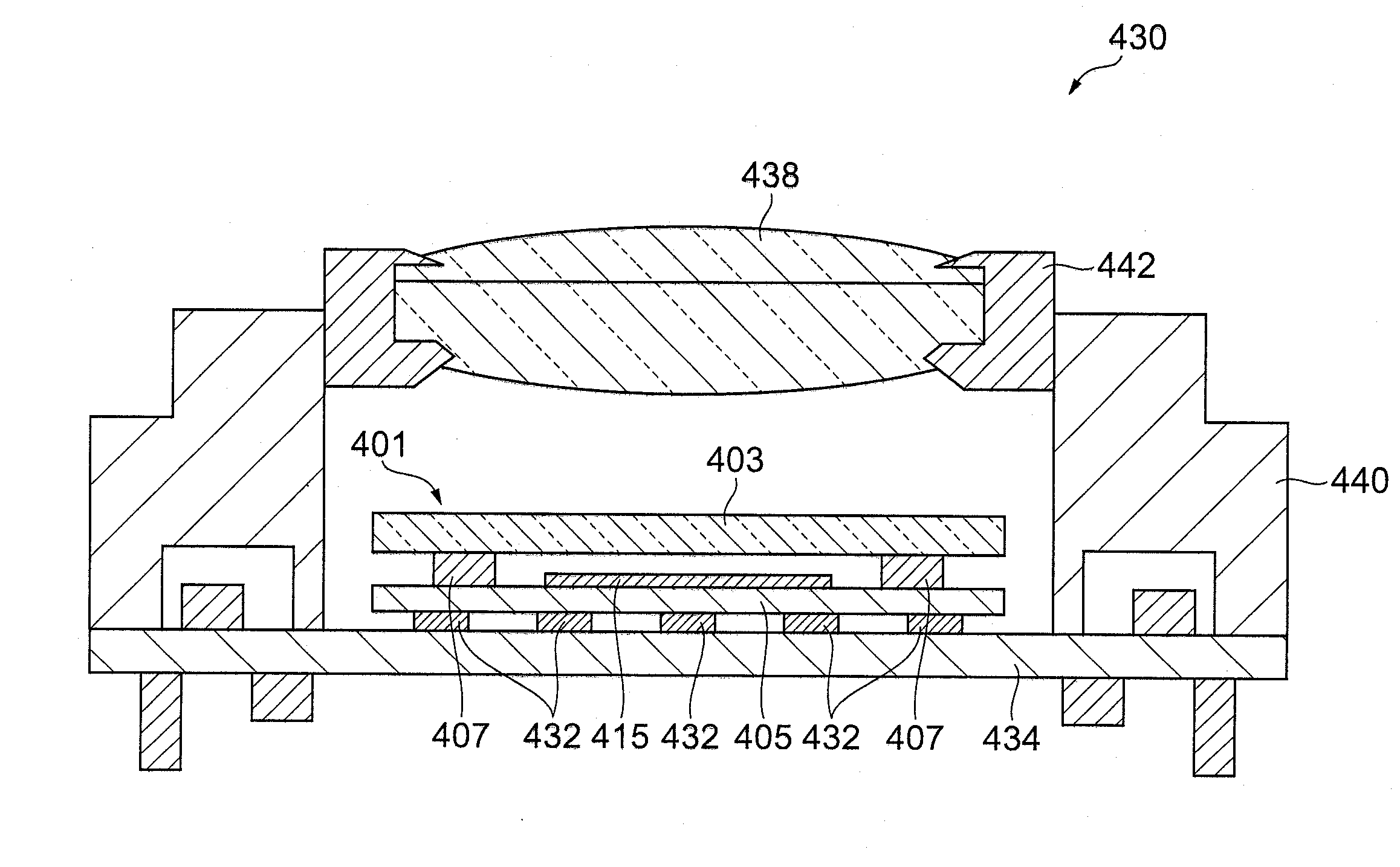
Photosensitive adhesive composition, photosensitive film adhesive, adhesive pattern, semiconductor wafer with adhesive, semiconductor device and electronic component
a technology of photosensitive film and composition, applied in the direction of film/foil adhesives, record information storage, synthetic resin layered products, etc., can solve the problems of difficult to achieve high levels for both pattern formability, high thermal damage to surrounding materials, and increased thermal stress, etc., to achieve high-yield production of semiconductor devices
- Summary
- Abstract
- Description
- Claims
- Application Information
AI Technical Summary
Benefits of technology
Problems solved by technology
Method used
Image

Examples
examples
[0211]The present invention will now be explained in detail by examples, with the understanding that the invention is not limited to the examples.
[0212]The starting materials listed in Table 1 were used to prepare polyimide resins PI-1 to PI-5.
TABLE 1PI-1PI-2PI-3PI-4PI-5Mono functional acidTAATAATAA——anhydrideTetracarboxylicODPAODPAODPAODPAODPAdianhydrideCarboxyl group-MBAAMBAAMBAAMBAAMBAAcontaining diamineDiamine withD-400D-400D-400D-400D-400propylene etherskeletonDiamine with——B-12—B-12ether skeletonDiamine withBY16-BY16-BY16-—BY16-siloxane skeleton871EG871EG871EG871EGThe compound names in Table 1 are as follows.D-400: Polyetherdiamine by BASF (molecular weight: 452.4)BY16-871EG: 1,3-bis(3-Aminopropyl)tetramethyldisiloxane by Dow Corning Toray (molecular weight: 248.51)MBAA: 5,5′-Methylene-bis(anthranilic acid) by Wakayama Seika (molecular weight: 286.3)ODPA: 4,4′-Oxydiphthalic dianhydride by Manac, Inc. (molecular weight: 326.2).TAA: Trimellitic anhydride by Mitsubishi Gas Chemic...
examples 1-5
, Comparative Examples 1-4
[0223]Each of the obtained polyimide varnishes (PI-1 to PI-5) were used for mixing of the components in the compositional ratios listed in Table 1 and Table 2 (units: parts by weight), to obtain photosensitive adhesive compositions (adhesive layer-forming varnishes).
TABLE 2Example12345Base polymerPI-1——100 ——PI-2———100 —PI-3100 100 ——100 Radiation-BPE-100——404040polymerizableA-93007070 30——compoundU-2PPA———40—M-313————30Epoxy resinVG-3101 55 5 5 5YDF-81703010 101010Curing agentTrisP-PA105 5 5 5FillerR-972——303030PhotoinitiatorI-819—1 3 3 3I-OXE02 32———Thermal radicalPERCUMYL D—— 2 2 2generator
TABLE 3Comp. Ex.1234Base polymerPI-4—100 ——PI-5100 —100 100 Radiation-BPE-10040 40 40 40 polymerizableA-930030 30 ——compoundU-2PPA——40 —M-313———30 Epoxy resinVG-31015555YDF-817010 10 10 10 Curing agentTrisP-PA5555FillerR-972—30 30 30 PhotoinitiatorI-8193333Thermal radicalPERCUMYL D2222generatorThe compound names in Table 2 and Table 3 are as follows.BPE-100: Ethoxylate...
PUM
| Property | Measurement | Unit |
|---|---|---|
| temperature | aaaaa | aaaaa |
| temperature | aaaaa | aaaaa |
| thickness | aaaaa | aaaaa |
Abstract
Description
Claims
Application Information