Surrounding stacked gate multi-gate fet structure nonvolatile memory device

a nonvolatile memory device and stacked gate technology, applied in the direction of semiconductor devices, transistors, electrical equipment, etc., can solve the problems of increased junction leakage current, short battery life, and increased leakage curren

Active Publication Date: 2011-07-07
SEMICON MFG INT (SHANGHAI) CORP +1
View PDF5 Cites 21 Cited by
  • Summary
  • Abstract
  • Description
  • Claims
  • Application Information

AI Technical Summary

Benefits of technology

[0007]The present invention is generally related to integrated circuit devices and methods of manufacturing semiconductor devices. More particularly, ...

Problems solved by technology

This causes a short channel effect and also increases the junction leakage current.
In a notebook computer, leakage current means short battery life and in a server computer, it means higher power bills.
Also, in a nonvolatile memory device, the leakage current leads to degradation of data retention time and other electrical characteristics as the device feature size is reduced.
However, depend...

Method used


Image

  • Surrounding stacked gate multi-gate fet structure nonvolatile memory device
  • Surrounding stacked gate multi-gate fet structure nonvolatile memory device
  • Surrounding stacked gate multi-gate fet structure nonvolatile memory device

Examples


Embodiment Construction

[0019]The present invention generally relates to integrated circuit devices and their processing for the manufacture of semiconductor devices. More particularly, the present invention provides a method for forming a surrounding stacked gate fin field effect transistor (fin FET) structure nonvolatile memory device.

[0020]Exemplary embodiments of the invention are more fully described in detail with reference to the accompanied drawings. The invention may be embodied in many different forms and should not be construed as being limited to the exemplary embodiments set forth herein. Rather, these exemplary embodiments are provided so that this disclosure is thorough and complete, and to convey the concepts of the invention to those skilled in the art.

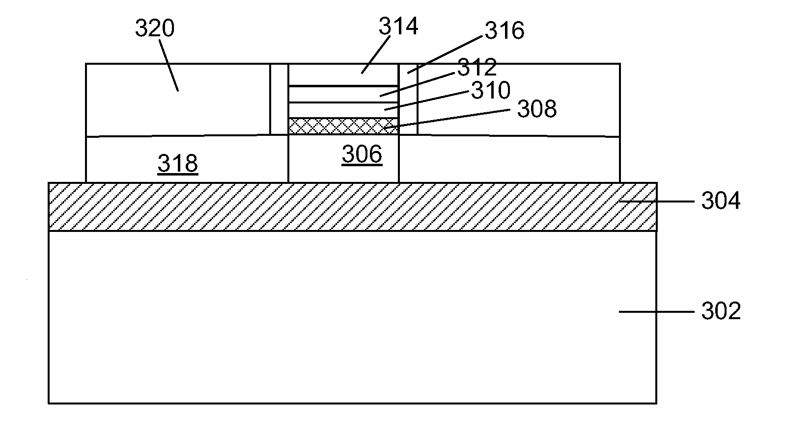
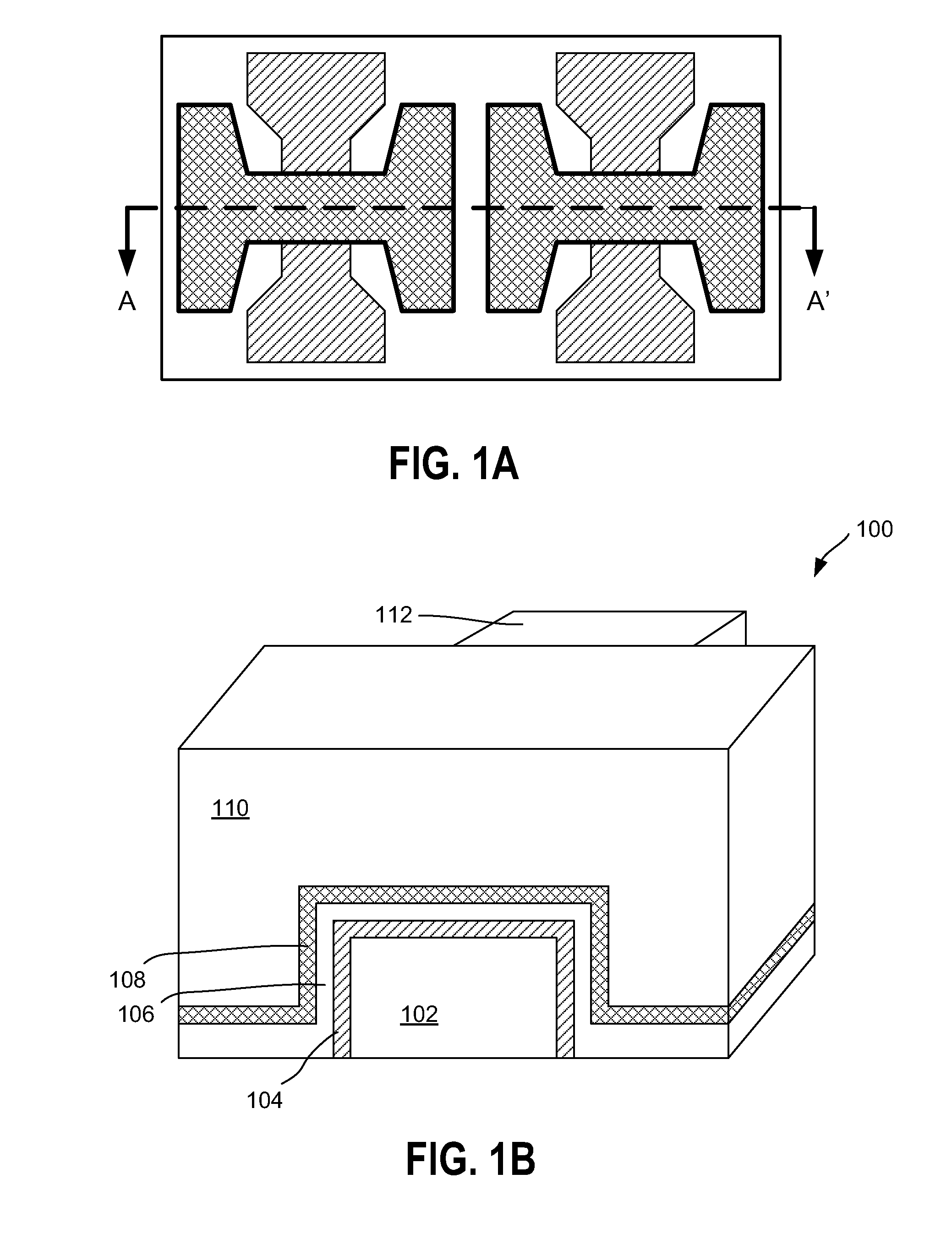
[0021]FIG. 1A is a simplified top view of a surrounding stacked gate fin FET structure non-volatile memory (NVM) device according to an embodiment of the present invention. This diagram is merely an example, which should not unduly limit the...


PUM


Abstract

Nonvolatile memory devices having a low off state leakage current and an excellent data retention time characteristics. The present invention provides a surrounding stacked gate fin field effect transistor nonvolatile memory structure comprising a silicon-on-insulator substrate of a first conductivity type and a fin active region projecting from an upper surface of the insulator. The structure further includes a tunnel oxide layer formed on the fin active region and a first gate electrode disposed on the tunnel oxide layer and upper surface of the insulator. Additionally, the structure includes an oxide/nitride/oxide (ONO) composite layer formed on the first gate electrode, a second gate electrode formed on the ONO composite layer and patterned so as to define a predetermined area of the ONO composite layer. The structure further includes a dielectric spacer formed on a sidewall of the second gate electrode and source/drain regions formed in the fin active region on both sides of the second gate electrode.

Description

CROSS-REFERENCES TO RELATED APPLICATIONS[0001]This application claims priority to Chinese Patent Application No. 200910057968.7, filed Sep. 28, 2009 by inventors Deyuan Xiao et al., commonly assigned and incorporated in its entirety by reference herein for all purposes.BACKGROUND OF THE INVENTION[0002]The present invention is generally related to integrated circuit devices and their processing for the manufacture of semiconductor devices. More particularly, the present invention provides a method for forming a surrounding stacked gate fin field effect transistor (fin FET) structure nonvolatile memory device.[0003]As semiconductor memory devices become increasingly integrated, the feature size including the channel length of individual devices is gradually reduced. This causes a short channel effect and also increases the junction leakage current. Leakage current was not a significant problem in the past, but it has become more serious concern now that transistor gates and other chip...

Claims


Application Information

Patent Timeline
IPC IPC(8): H01L29/788H01L21/336
CPCH01L21/28273H01L21/845H01L27/11521H01L29/66825H01L29/42324H01L29/785H01L29/7881H01L27/1211H01L29/40114H10B41/30
Inventor XIAO, DEYUANJIANG, LILYCHEN, GARYLEE, ROGER
Owner SEMICON MFG INT (SHANGHAI) CORP
Why Eureka
Try Eureka