Semiconductor device manufacturiing method

Active Publication Date: 2011-08-25
TOYOTA JIDOSHA KK +1
View PDF7 Cites 62 Cited by
  • Summary
  • Abstract
  • Description
  • Claims
  • Application Information

AI Technical Summary

Benefits of technology

[0006]In addition, if the lower surface structure formation step is carried out prior to the upper surface structure formation step, this means that a lower surface electrode is formed prior to forming a surface cover film made of polyimide, for example, formed on the upper surface of the semiconductor device, thereby increasing susceptibility to contamination of the contact interface between the upper surface electrode and the semiconductor substrate.
[0007]An object of the present teachings is to realize both a protection of upper surface structures such as the upper surface electrode formed on the upper surface of the semiconductor device and a making the ohmic contact between the lower surface electrode and the semiconductor substrate by protecting upper surface structures such as the upper surface electrode formed on the upper surface of the semiconductor device even if the silicon carbide semiconductor device is manufactured by a manufacturing method in which the upper surface structure formation step is carried out prior to the lower surface structure formation step.
[0009]In the above-mentioned manufacturing method, in the annealing step (b2) included in the step (b), the ohmic contact is made between the lower surface electrode material layer and the semiconductor substrate by irradiating the lower surface electrode material layer with laser. Since the laser radiation is used, the upper surface structures already formed on the upper surface of the semiconductor substrate are not subjected to damage by contamination and the like in the annealing step (b2). Consequently, if the step (b) that includes the annealing step (b2) is carried out after the step (a) that includes the annealing step (a2), the ohmic contact can be ensured between the lower surface electrode and the semiconductor substrate of the silicon carbide semiconductor device.

Problems solved by technology

If the step of thinning the semiconductor wafer is carried out prior to the lower surface structure formation step and the upper surface structure formation step, the wafer that has been thinned must be transported in a subsequent step, thereby making the wafer increasingly susceptible to damage.
In addition, if the lower surface structure formation step is carried out prior to the upper surface structure formation step, this means that a lower surface electrode is formed prior to forming a surface cover film made of polyimide, for example, formed on the upper surface of the semiconductor device, thereby increasing susceptibility to contamination of the contact interface between the upper surface electrode and the semiconductor substrate.

Method used


Image

  • Semiconductor device manufacturiing method
  • Semiconductor device manufacturiing method
  • Semiconductor device manufacturiing method

Examples


first embodiment

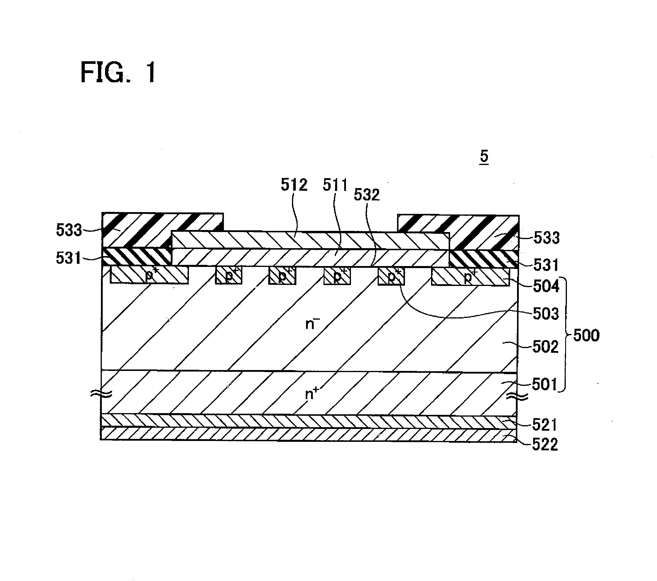
[0031]The following provides an explanation of a first embodiment of the present teachings with reference to the drawings. FIG. 1 is a drawing schematically showing a cross-section of a semiconductor device 5 manufactured according to a first manufacturing method relating to the first embodiment. The semiconductor device 5 is a diode having a Junction Barrier Schottky (JBS) structure. A semiconductor substrate 500 is provided with an n-type substrate layer 501 having silicon carbide as a material thereof, an n+-type epitaxial layer 502 laminated on the surface of the substrate layer 501 and having silicon carbide as a material thereof, and a p+-type anode layer 503 and p+-type blocking layer 504 provided on the surface of the epitaxial layer 502. The anode layer 503 is an anode layer having a JBS structure, while the blocking layer 504 employs a Junction Terminal Extension (JTE) structure provided as a peripheral blocking structure.

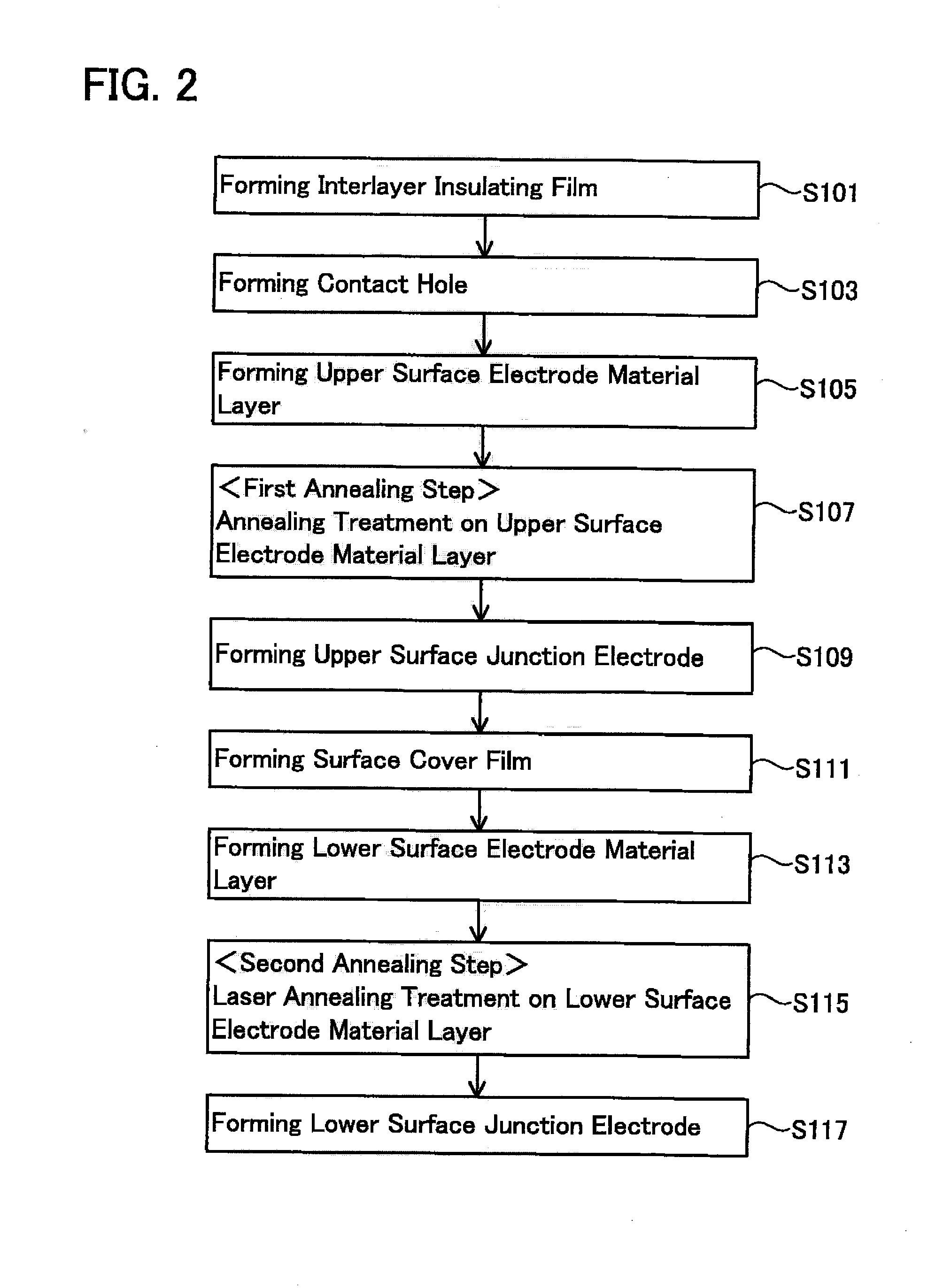
[0032]An interlayer insulating film 531, an upper s...

example 1

[0075]The following provides a more detailed explanation of an Example 1 that embodies the first embodiment as described above.

[0076](Preparation of Raw Material Wafer)

[0077]An n−-type epitaxial layer (impurity concentration: 5×1015 cm−3, layer thickness: 10 μm) was deposited on the upper surface of a 4H—SiC n+-type semiconductor wafer (impurity concentration: 8×1018 cm−3) having a diameter of 100 mm and thickness of 350 μm. This semiconductor wafer is equivalent to the substrate layer 501 shown in FIG. 1, and this epitaxial layer is equivalent to the epitaxial layer 502 shown in FIG. 1. Moreover, Al ions were injected into the upper surface of the epitaxial layer for forming a p+-type JTE structure, after which Al ions were injected into the upper surface of the epitaxial layer for forming a p+-type JBS structure. Subsequently, annealing was carried out to form the p+-type JTE structure (impurity concentration: 1×1019 cm−3, width: 50 μm, depth: 1 μm) and the p+-type JBS structure (...

second embodiment

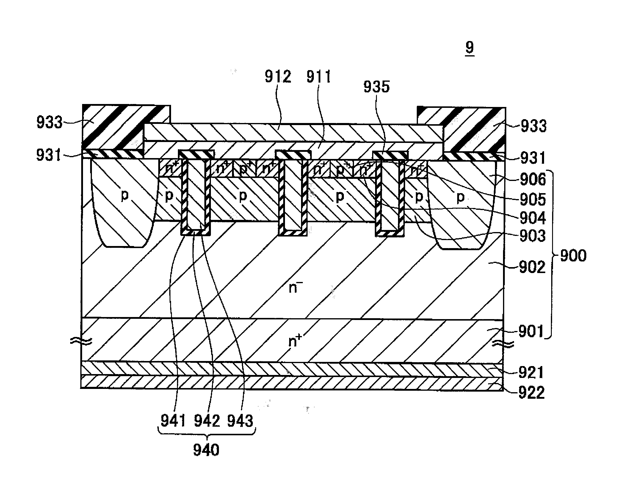
[0109]A semiconductor device capable of being manufactured according to the manufacturing method relating to the present teachings may be a semiconductor device having an upper surface electrode in contact with the upper surface of the semiconductor substrate and a lower surface electrode in contact with the lower surface of the semiconductor substrate. An explanation of the second embodiment is provided using as an example a MOSFET shown in FIG. 5 as an example of the semiconductor device alternative to the diode explained in the first embodiment.

[0110]FIG. 5 is a drawing schematically showing a cross-section of a semiconductor device 9 manufactured according to a second manufacturing method relating to the second embodiment. The semiconductor device 9 is a MOSFET. A semiconductor substrate 900 is provided with an n-type drain layer 901, having as a material thereof a semiconductor substrate having silicon carbide as a material thereof, a drift layer 902 laminated on the upper surf...


PUM

PropertyMeasurementUnit
Temperatureaaaaaaaaaa
Thicknessaaaaaaaaaa
Thicknessaaaaaaaaaa

Abstract

A method for manufacturing a semiconductor device including a semiconductor substrate composed of silicon carbide, an upper surface electrode which contacts an upper surface of the substrate, and a lower surface electrode which contacts a lower surface of the substrate, the method including steps of: (a) forming an upper surface structure on the upper surface side of the substrate, and (b) forming a lower surface structure on the lower surface side of the substrate. The step (a) comprises steps of: (a1) depositing an upper surface electrode material layer on the upper surface of the substrate, the upper surface electrode material layer being a raw material layer of the upper surface electrode, and (a2) annealing the upper surface electrode material layer. The step (b) comprises steps of: (b1) depositing a lower surface electrode material layer on the lower surface of the substrate, the lower surface electrode material layer being a raw material layer of the lower surface electrode, and (b2) annealing the lower surface electrode material layer with a laser to make an ohmic contact between the lower surface electrode and the substrate.

Description

CROSS-REFERENCE TO RELATED APPLICATION[0001]This application claims priority to Japanese Patent Application No. 2010-034595 filed on Feb. 19, 2010, the contents of which are hereby incorporated by reference into the present application.TECHNICAL FIELD[0002]The present application relates to a method for manufacturing a semiconductor device from a semiconductor wafer composed of silicon carbide.DESCRIPTION OF RELATED ART[0003]In a semiconductor device provided with a substrate having silicon carbide (SiC) as a material thereof (to be referred to as a silicon carbide semiconductor device), an electrode that forms a Schottky bather junction with the semiconductor substrate may be used for an upper surface electrode, while an electrode that makes an ohmic contact with the semiconductor substrate may be used for a lower surface electrode. In this case, temperature at which the lower surface electrode is heat-treated is higher than temperature at which the upper surface electrode is heat-...

Claims


Application Information

Patent Timeline
IPC IPC(8): H01L21/28C21D1/09
CPCC21D1/09H01L29/872H01L21/0445H01L21/0485H01L21/0495H01L21/268H01L21/67115H01L29/0615H01L29/0619H01L29/1095H01L29/1608H01L29/45H01L29/47H01L29/6606H01L29/66068H01L29/7811H01L29/7813C22F1/10H01L21/324
Inventor FUJIWARA, HIROKAZUKONISHI, MASAKIKAWAI, JUNYAMAMOTO, TAKEOENDO, TAKESHIKATSUNO, TAKASHIWATANABE, YUKIHIKOSOEJIMA, NARUMASA
Owner TOYOTA JIDOSHA KK
Why Eureka
Try Eureka