Semiconductor device

a semiconductor and device technology, applied in semiconductor devices, instruments, electrical equipment, etc., can solve problems such as connection failure, short-channel effect problems, and serious problems generated in the manufacturing process, so as to reduce the variation in the electrical characteristics of transistors across the substrate plane, reduce the thickness of the second conductive layer, and reduce the contact area

Active Publication Date: 2011-09-01
SEMICON ENERGY LAB CO LTD
View PDF34 Cites 27 Cited by
  • Summary
  • Abstract
  • Description
  • Claims
  • Application Information

AI Technical Summary

Benefits of technology

[0034]By the above effects, the problems which are caused due to miniaturization are solved. As a result, it is possible to sufficiently reduce the size of a transistor. By sufficiently reducing the size of a transistor, the area occupied by a semiconductor device is reduced and the number of semiconductor devices which can be manufactured using one substrate is increased. Accordingly, the manufacturing cost per semiconductor device is suppressed. Further, the size of the semiconductor device can be reduced without its function degrading; therefore, the semiconductor device of the same size can have improved functions. Moreover, advantageous effects such as high-speed operation and low power consumption due to a reduction in channel length can be obtained. In other words, according to one embodiment of the disclosed invention, miniaturization of a transistor including an oxide semiconductor is achieved, and a variety of advantageous effects accompanying it can be obtained.
[0035]Further, by forming the sidewall insulating layer including different material layers in the transistor, variation in the thickness of the second conductive layer can be reduced. This can reduce variation in the contact area between the second conductive layer and the oxide semiconductor layer, and thus variation in electrical characteristics of transistors across the substrate plane can be reduced.
[0036]As described above, according to one embodiment of the disclosed invention, a semiconductor device which suppresses defects or maintains favorable characteristics, and achieves miniaturization can be provided.

Problems solved by technology

In miniaturization of a transistor, a defect generated in the manufacturing process becomes a serious problem.
For example, although a source electrode, a drain electrode, and a channel formation region should be electrically connected, breakage, connection failure, or the like may occur due to a reduction in coverage by the miniaturization.
Further, in miniaturization of a transistor, a short-channel effect becomes problematic.

Method used


Image

  • Semiconductor device
  • Semiconductor device
  • Semiconductor device

Examples


embodiment 1

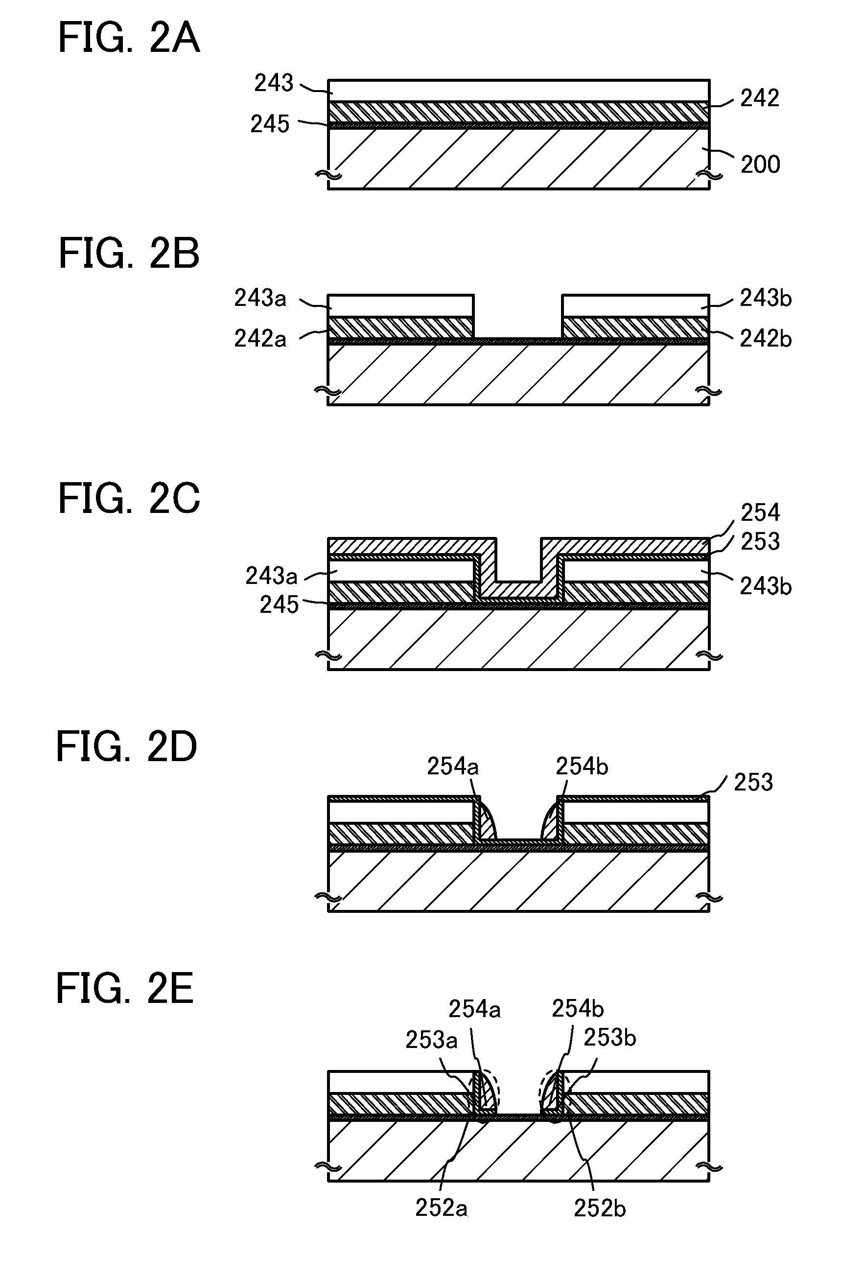
[0048]In this embodiment, an example of a structure of a semiconductor device and a manufacturing process according to one embodiment of the disclosed invention will be described with reference to FIG. 1, FIGS. 2A to 2D, FIGS. 3A to 3D, and FIGS. 4A to 4C.

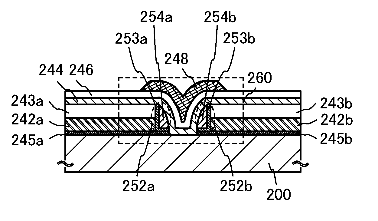
[0049]FIG. 1 illustrates a cross-sectional structure of a transistor as an example of a semiconductor device. FIG. 1 illustrates a top-gate transistor as a transistor according to one embodiment of the disclosed invention.

[0050]A transistor 260 illustrated in FIG. 1 includes, over a substrate 200, a source electrode in which a second conductive layer 245a and a first conductive layer 242a are sequentially stacked, a drain electrode in which a second conductive layer 245b and a first conductive layer 242b are sequentially stacked, a sidewall insulating layer 252a in contact with the source electrode, a sidewall insulating layer 252b in contact with the drain electrode, an insulating layer 243a over the source electrode, an insulatin...

modification example

[0115]Next, modified examples of the semiconductor device illustrated in FIG. 1 will be described with reference toFIGS. 4A to 4C.

[0116]A transistor 270 illustrated in FIG. 4A has a structure partly different from the structure of the transistor 260 illustrated in FIG. 1.

[0117]The transistor 270 illustrated in FIG. 4A has a sidewall insulating layer 252c and a sidewall insulating layer 252d. The sidewall insulating layer 252c includes an insulating layer 254c the length of a bottom surface of which in the channel length direction is shorter than the length (LS1) of an extended region of the insulating layer 253a. The sidewall insulating layer 252d includes an insulating layer 254d the length of a bottom surface of which in the channel length direction is shorter than the length (LD1) of an extended region of the insulating layer 253b.

[0118]A manufacturing method of the transistor 270 illustrated in FIG. 4A is described. After the steps illustrated in FIGS. 2A to 2E and FIG. 3A are ...

embodiment 2

[0129]In this embodiment, application examples of a semiconductor device according to one embodiment of the disclosed invention will be described with reference to FIGS. 5A to 5C. Here, an example of a memory device will be described. Note that in each of the circuit diagrams, “OS” may be written beside a transistor in order to indicate that the transistor includes an oxide semiconductor.

[0130]In the semiconductor device in FIG. 5A, a first wiring (a 1st line) and a source electrode of a transistor 300 are electrically connected to each other, and a second wiring (a 2nd line) and a drain electrode of the transistor 300 are electrically connected to each other. In addition, a gate electrode of the transistor 300 and one of a source electrode and a drain electrode of a transistor 310 are electrically connected to one electrode of a capacitor 320, a third wiring (a 3rd line) and the other of the source electrode and the drain electrode of the transistor 310 are electrically connected t...


PUM


Abstract

A semiconductor device includes an oxide semiconductor layer, a source electrode and a drain electrode in contact with the oxide semiconductor layer, a gate electrode overlapping with the oxide semiconductor layer, and a gate insulating layer between the oxide semiconductor layer and the gate electrode, in which the source electrode or the drain electrode comprises a first conductive layer and a second conductive layer having a region which extends beyond an end portion of the first conductive layer in a channel length direction and which overlaps with part of the gate electrode, in which a sidewall insulating layer is provided over the extended region of the second conductive layer, and in which the sidewall insulating layer comprises a stack of a plurality of different material layers.

Description

TECHNICAL FIELD[0001]A technical field of the present invention relates to a semiconductor device. Note that a semiconductor device herein refers to elements and devices in general which function by utilizing semiconductor characteristics.BACKGROUND ART[0002]There are a wide variety of metal oxides and such metal oxides are used for various applications. Indium oxide is a well-known material and has been used as a transparent electrode material which is necessary in liquid crystal display devices or the like.[0003]Some metal oxides have semiconductor characteristics. The examples of such metal oxides having semiconductor characteristics are tungsten oxide, tin oxide, indium oxide, zinc oxide, and the like. A thin film transistor in which a channel formation region is formed using such metal oxide has been already known (for example, see Patent Documents 1 to 4, Non-Patent Document 1, and the like).[0004]As metal oxides, not only single-component oxides but also multi-component oxide...

Claims


Application Information

Patent Timeline
Patent Type & Authority Applications(United States)
IPC IPC(8): H01L29/78
CPCG11C16/0408G11C16/0483H01L27/11521H01L29/66969H01L29/41733H01L29/45H01L29/7869H01L27/1156H10B41/70H10B41/30H01L27/1225H01L29/66742
Inventor SUZAWA, HIDEOMISASAGAWA, SHINYAKURATA, MOTOMU
Owner SEMICON ENERGY LAB CO LTD
Why Eureka
Try Eureka