Semiconductor device and method for manufacturing semiconductor device

Inactive Publication Date: 2011-09-08
SEMICON ENERGY LAB CO LTD
View PDF99 Cites 57 Cited by
  • Summary
  • Abstract
  • Description
  • Claims
  • Application Information

AI Technical Summary

Benefits of technology

[0041]As described above, according to one embodiment of the disclosed invention, a semiconductor device which

Problems solved by technology

In the case where a transistor is miniaturized, a defect generated in the manufacturing process becomes a major problem.
For example, in a transistor where a semiconductor layer is formed over a wiring functioning as a source or drain electrode, a gate electrode or the like, the wiring has a larger thickness than the semiconductor layer, which causes poor coverage with the semiconductor layer when the thickness of the semiconduc

Method used


Image

  • Semiconductor device and method for manufacturing semiconductor device
  • Semiconductor device and method for manufacturing semiconductor device
  • Semiconductor device and method for manufacturing semiconductor device

Examples


embodiment 1

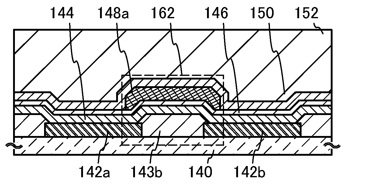
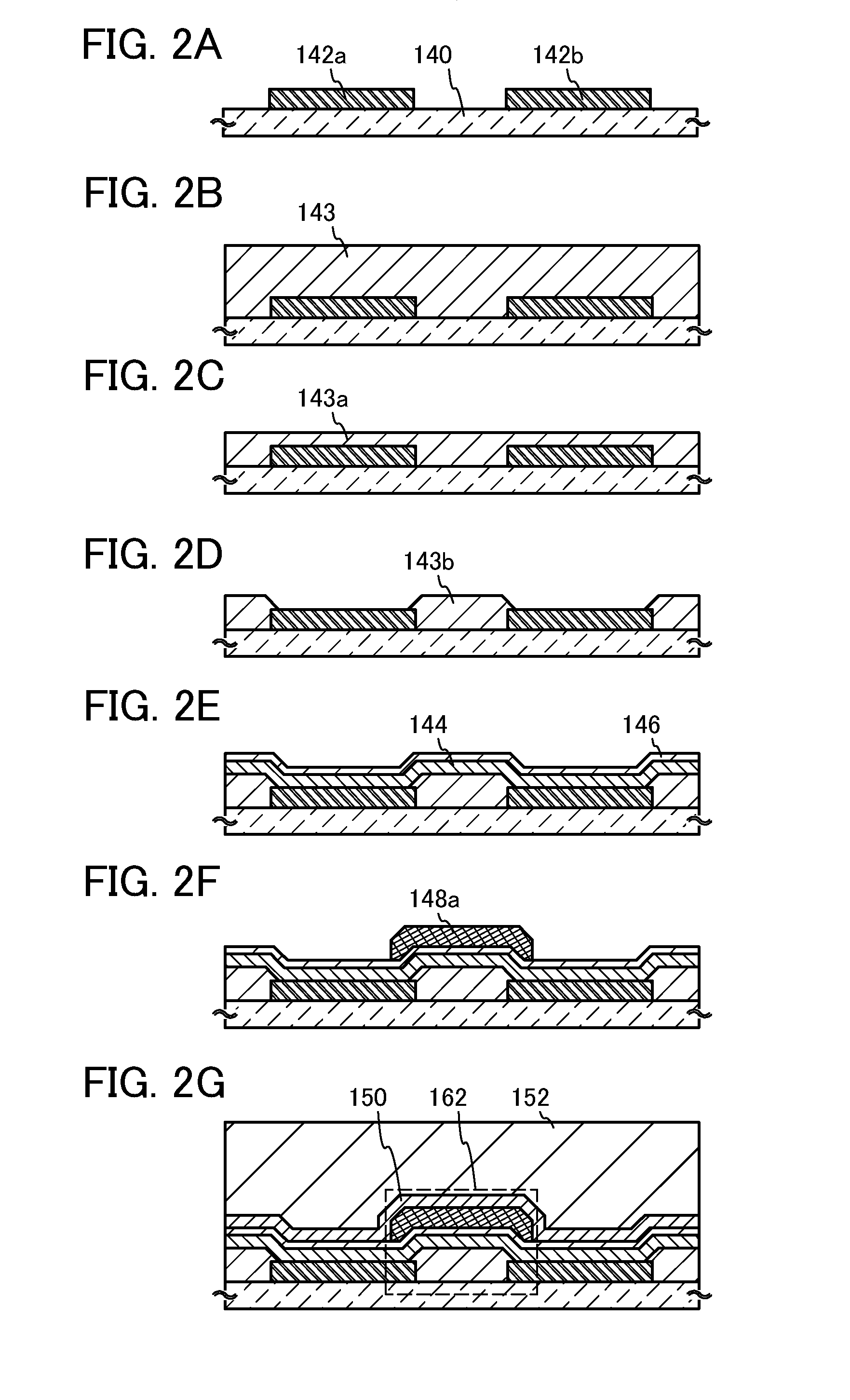
[0063]In this embodiment, a structure and a manufacturing method of a semiconductor device according to one embodiment of the disclosed invention will be described with reference to FIGS. 1A to 1C, FIGS. 2A to 2G, and FIGS. 3A to 3G

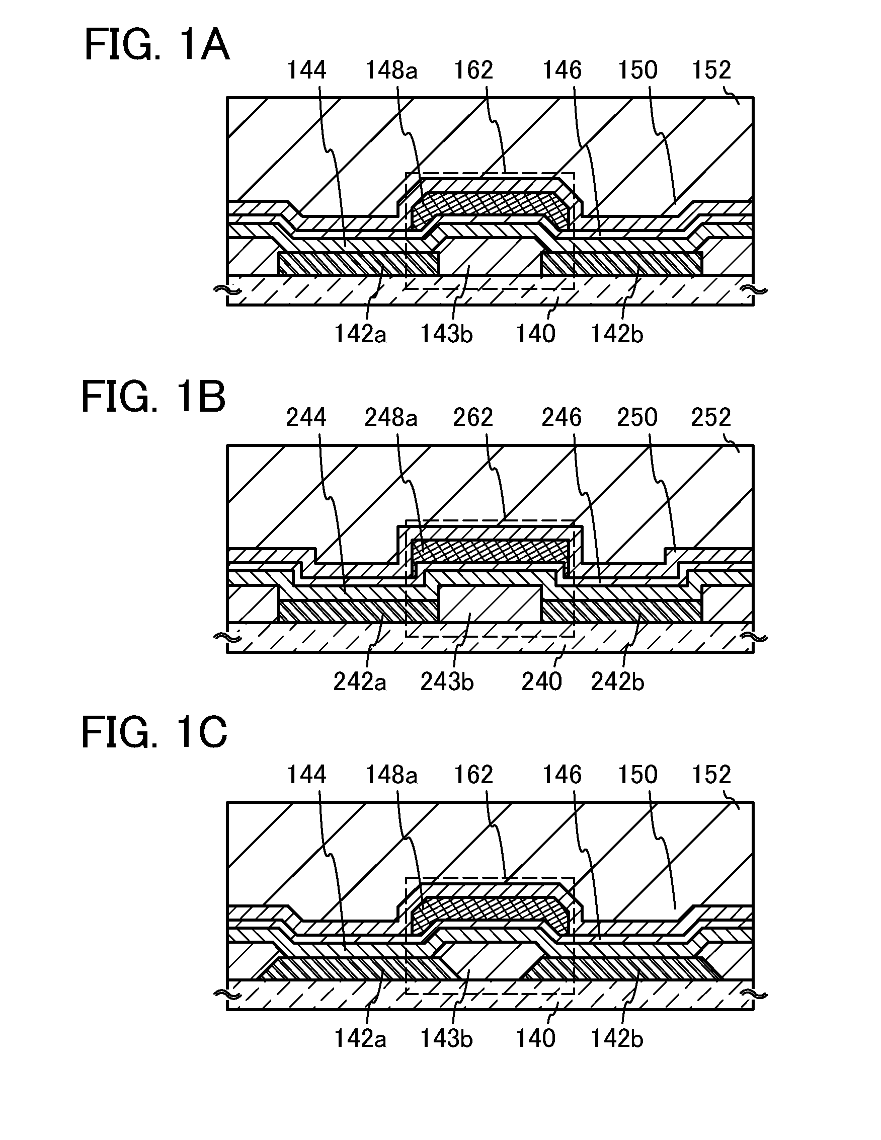
[0064]FIGS. 1A to 1C each illustrate an example of a structure of a semiconductor device. FIG. 1A is a first structural example, and FIG. 1B is a second structural example. FIG. 1C is a modified example of FIG. 1A.

[0065]A transistor 162 in FIG. 1A includes an insulating layer 143b over a substrate 140 having a surface where components are formed, a source electrode 142a and a drain electrode 142b embedded in an insulating layer including the insulating layer 143b, an oxide semiconductor layer 144 in contact with part of an upper surface of the insulating layer 143b, an upper surface of the source electrode 142a, and an upper surface of the drain electrode 142b, a gate insulating layer 146 covering the oxide semiconductor layer 144, and a gate electrode 14...

embodiment 2

[0141]In this embodiment, a structure and a manufacturing method of a semiconductor device according to another embodiment of the disclosed invention will be described with reference to FIGS. 4A to 4C, FIGS. 5A to 5D, and FIGS. 6A to 6C. Note that in some circuit diagrams mentioned below, “OS” is written beside a transistor in order to indicate that the transistor includes an oxide semiconductor.

[0142]FIGS. 4A to 4C illustrate an example of a structure of a semiconductor device. FIG. 4A is a cross-sectional view of the semiconductor device; FIG. 4B is a plan view of the semiconductor device; and FIG. 4C illustrates a circuit configuration of the semiconductor device. Note that a structure of the semiconductor device is mainly described in this embodiment, and operation of the semiconductor device will be described in detail in an embodiment below. Note that the semiconductor device illustrated in FIGS. 4A to 4C is just an example having predetermined functions and does not represent...

embodiment 3

[0174]In this embodiment, an example of application of a semiconductor device according to one embodiment of the disclosed invention will be described with reference to FIGS. 7A-1, 7A-2, and 7B. Here, an example of a memory device is described. Note that in some circuit diagrams mentioned below, “OS” is written beside a transistor in order to indicate that the transistor includes an oxide semiconductor.

[0175]In a semiconductor device which can be used as a memory device, which is illustrated in FIG. 7A-1, a first wiring (1st Line) is electrically connected to a source electrode of a transistor 1000. A second wiring (2nd Line) is electrically connected to a drain electrode of the transistor 1000. A third wiring (3rd Line) is electrically connected to one of a source electrode and a drain electrode of a transistor 1010. A fourth wiring (4th Line) is electrically connected to a gate electrode of the transistor 1010. Furthermore, a gate electrode of the transistor 1000 and the other of ...


PUM


Abstract

Disclosed is a semiconductor device including an insulating layer, a source electrode and a drain electrode embedded in the insulating layer, an oxide semiconductor layer in contact with the insulating layer, the source electrode, and the drain electrode, a gate insulating layer covering the oxide semiconductor layer, and a gate electrode over the gate insulating layer. The upper surface of the surface of the insulating layer, which is in contact with the oxide semiconductor layer, has a root-mean-square (RMS) roughness of 1 nm or less. There is a difference in height between an upper surface of the insulating layer and each of an upper surface of the source electrode and an upper surface of the drain electrode. The difference in height is preferably 5 nm or more. This structure contributes to the suppression of defects of the semiconductor device and enables their miniaturization.

Description

TECHNICAL FIELD[0001]The present invention relates to a semiconductor device and a manufacturing method thereof. Note that semiconductor devices herein refer to general elements and devices which function by utilizing semiconductor characteristics.BACKGROUND ART[0002]There are a wide variety of metal oxides and such metal oxides are used for various applications. Indium oxide is a well-known material and is used as a material for transparent electrodes which are needed for liquid crystal display devices or the like.[0003]Some metal oxides have semiconductor characteristics. Examples of such metal oxides having semiconductor characteristics include tungsten oxide, tin oxide, indium oxide, zinc oxide, and the like. A thin film transistor in which a channel formation region is formed using such a metal oxide has been already known (see, for example, Patent Documents 1 to 4, Non-Patent Document 1, and the like).[0004]Examples of metal oxides include not only a single-component oxide but...

Claims


Application Information

Patent Timeline
IPC IPC(8): H01L27/088H01L29/78H01L21/34H01L21/8254
CPCH01L27/1225G06F15/7832H01L29/1033H01L29/7869H01L29/41733H01L29/78603H01L29/78636
Inventor YAMAZAKI, SHUNPEIGODO, HIROMICHI
Owner SEMICON ENERGY LAB CO LTD
Why Eureka
Try Eureka